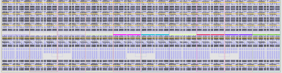
A 2000 LUT configuration, implemented with Openlane
Here is the first implementation of the S3GA<N=2048,M=8,K=4> design, which fits in the efabless Open Shuttle Program‘s ~10mm2caravel_user_project area (2.92mm x 3.52mm) for the 130nm Skywater PDK, as produced by the wonderful OpenLane tools.
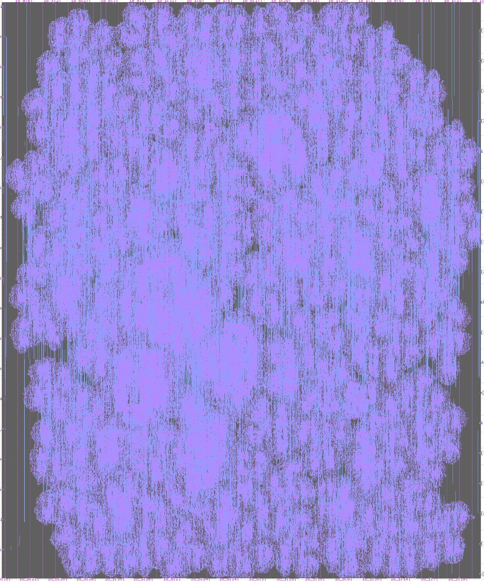
GDS-II plot of the first version of the S3GA<2048> design, implemented in 130nm sky130 process.
Implementation plus signoff checks take about 7 hours. At peak the tools used 60 GB of RAM. There are 2 wee Magic design rule check failures to investigate. Some design stats: 141,000 DFFs, 14,000 mux4s and 19,000 mux2s. This first cut has a 9 ns clock period = M=8-cycles at 72 ns = 14 MHz.
Next: DFFRAM?
This design uses 256-4=252 eight 4-LUT logic blocks (LB8s) (see part one), each of which uses an 8x48b configuration memory — an 8-entry x 48b circular shift register.
I hope to replace the hundreds of 8x configuration memories with bespoke, placed (floorplanned) instances of DFFRAM macros. This should also make it more practical to add a LUT-RAM mode to LB8s, so they may also be used as true dual port 32×8 SRAMs and possibly as 2R1W-64×4 SRAMs. Thus each X32 tile could implement a 32×32 register file.
It should also be possible to replace some X128 tiles with 100% DFFRAM or OpenRAM based block RAM (BRAM) cells at >3x the density of S3GA LUT-RAM.
Note: this blog post is under construction. This notice will be removed when it is complete.
Introduction: a look back at S4GA
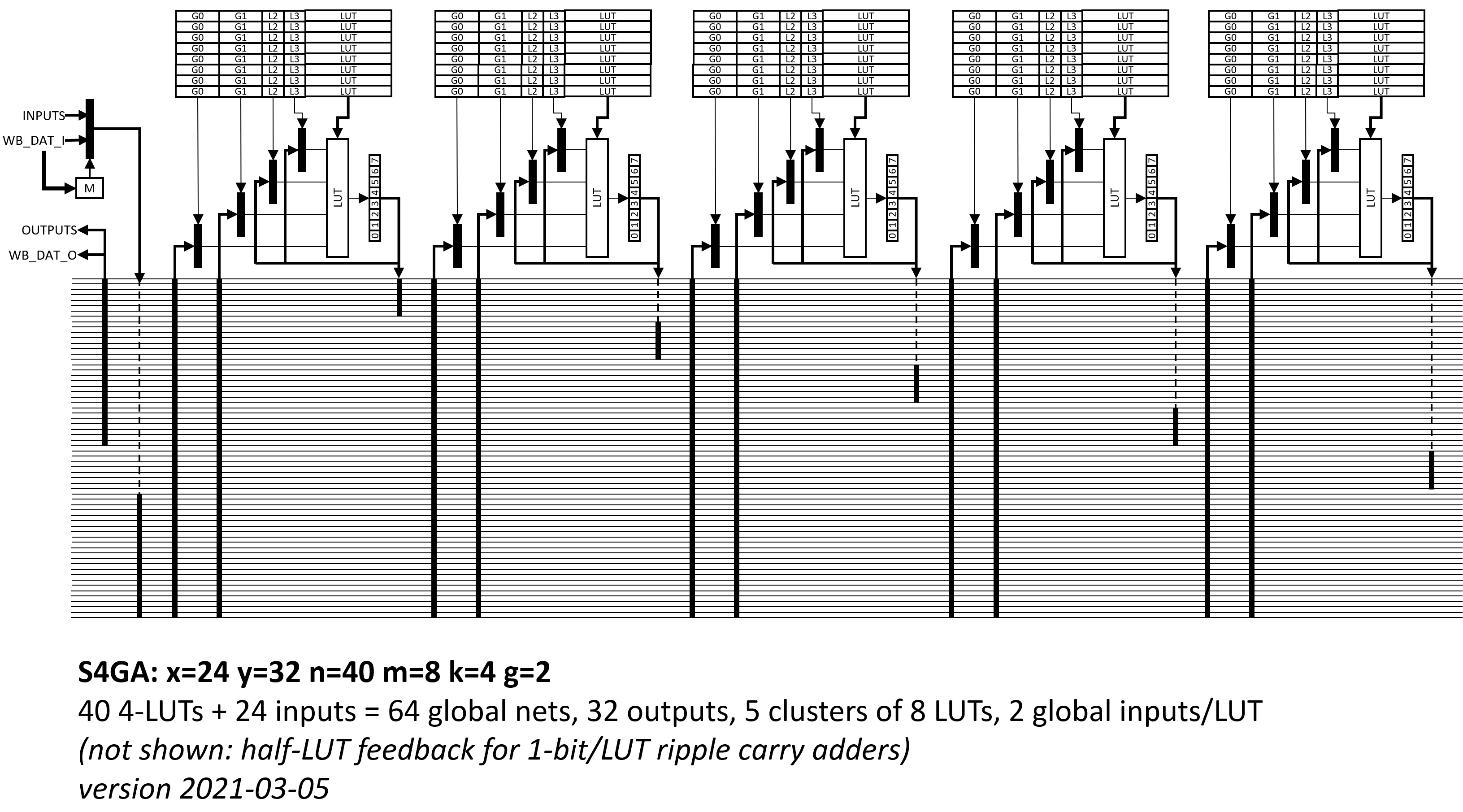
In winter 2021 I took the first edition of Matthew Venn’s superb Zero to ASIC course. My 300x300um project was S4GA: “a small simple slow serial” FPGA core, targeting ~0.1mm2 of the 130nm Skywater ASIC PDK, using the efabless Caravel harness and the Zero-to-ASIC multiproject framework. This core fit an N=40 4-LUT (four input lookup table) FPGA arranged in 5 clusters of M=8 LUTs, with a full cluster cycle time of M=8 cycles. A family tragedy interrupted this work and I did not finish it nor submit to MPW-1.
Block diagram of the N=40 M=8 K=4-LUT S4GA FPGA designed for the Zero-to-ASIC course (2021)
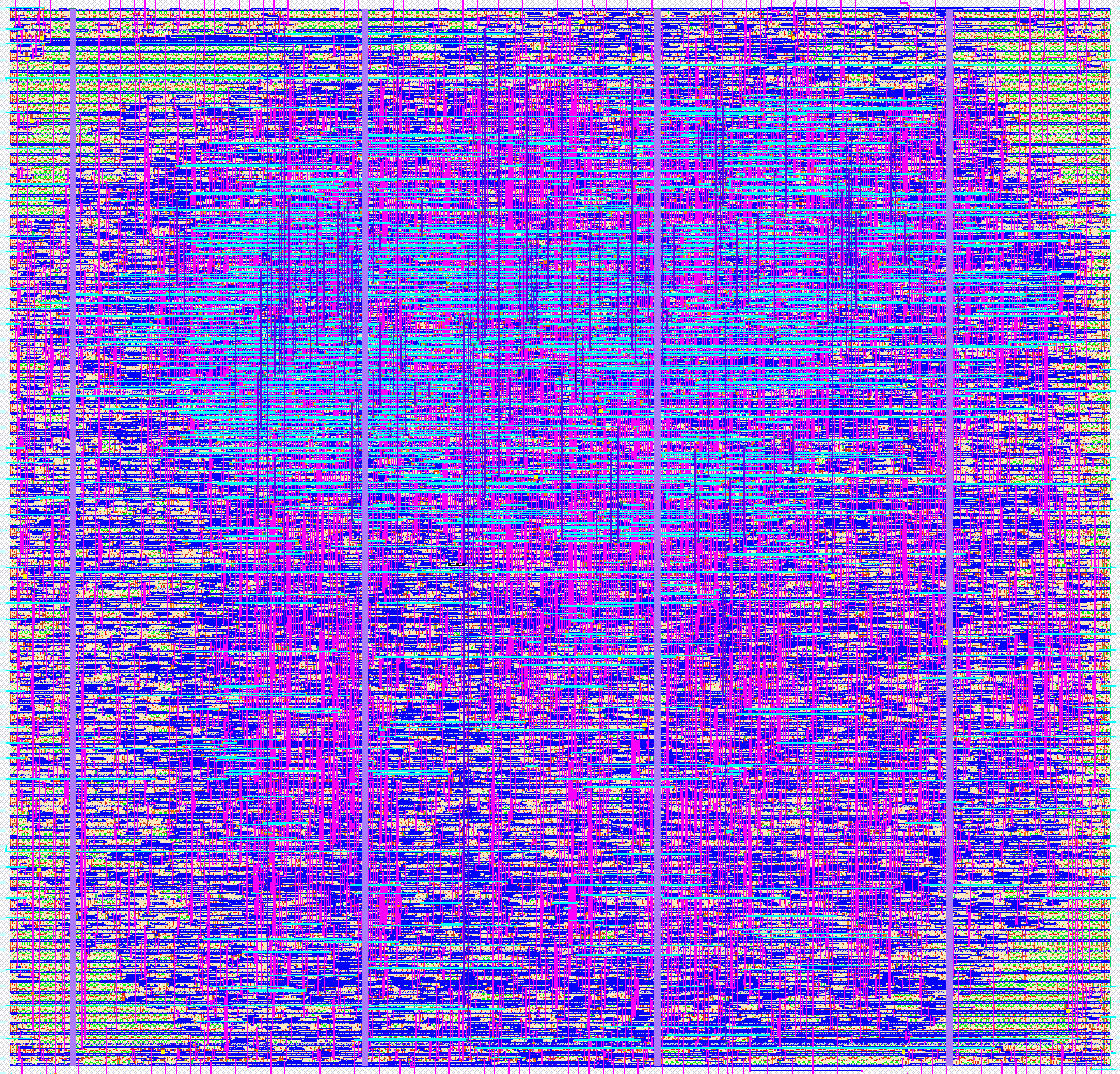
GDS plot (300um x 300um) of the Skywater130 implementation of the S4GA core, N=40 M=8 K=4-LUTs
Scaling way up with S3GA
Now I am reworking S4GA into a much larger (N>1000 LUTs) FPGA for the upcoming efablessMPW-8 run, closing Dec. 31, 2022. A full efabless Caravel user project area is over 10mm2, approximately 100x larger than this earlier N=40 design.
As this new FPGA core won’t be small, nor (in the spatial computation sense) slow, it is reborn as S3GA — simple scalable serial FPGA. (Pronounced “see-gah”, not “say-gah”.)
“What do you mean by serial FPGA?” The FPGA evaluates N logical LUTs using only N/M real LUTs, over M cycles. A serial FPGA trades off latency (e.g., logical clock period) for greater capacity by sharing (amortizing) the gate and wiring area of lookup table input and output multiplexers (muxes).
For S3GA, one LUT Block of M=8 logical K=4-LUTs (“LB8”) contains eight 4-LUT contexts (each about 40b, see below), and one physical 4-LUT (including one or more logic block input muxes, four LUT input muxes, one 16:1 LUT output mux, and a flip-flop output mux).
The README of the old N=40 S4GA design is instructive. Take a look. For that design:
N=40 and M=8, so across the whole design, this S4GA configuration evaluates 5 LUTs per cycle, or 40 LUTs per 8 cycles.
The global interconnect is just a flat 64b bus that passes each cluster. Each cluster has G=2 64:1 muxes to select two global input nets per LUT per clock.
Contemplating S3GA, with perhaps 50x more more LB8s and LUT outputs, this flat global interconnect architecture will not scale. For example, it could mean running 1000-bit buses past hundreds of LB8s and many hundreds of 1000:1 input muxes, and so forth. Such a flat design would also be over-provisioned with so many mm2 of unneeded global wiring and super wide LUT input muxes.
Rent’s Rule, T=tgp, estimates T (number of external IOs) as a function of g (number of gates), t and p constants, p<1, sometimes p=~0.5. It reflects that most of a circuit’s sub-circuits’ nets remain local to that sub-circuit — recursively so in a hierarchical design. For an FPGA architecture that hosts real world N LUT digital circuits, tNp global nets, instead of N global nets, will usually suffice. Also, within any subset of M k-LUTs of a circuit, there are never more than Mk inputs and M outputs.
Connecting a hierarchy of clusters
Instead of a classic island-style FPGA of rows and columns of M k-LUT clusters and switchboxes, S3GA will be a hierarchy of LB8s, clusters of LB8s, etc., interconnected with a hierarchy of switches in a fat tree like interconnect. This should allow a relatively simple place-and-route CAD flow to transform synthesized, technology mapped K-LUT netlists into S3GA configuration bitstreams.
Anticipating a 2D physical design layout, we arbitrarily pick a sub-cluster branch factor of four, so that sub-clusters may be (recursively) floorplanned to NW, NE, SW, SE quadrants of each cluster.
Here’s a sketch of a N=512 logical LUT quadrant of such a design:
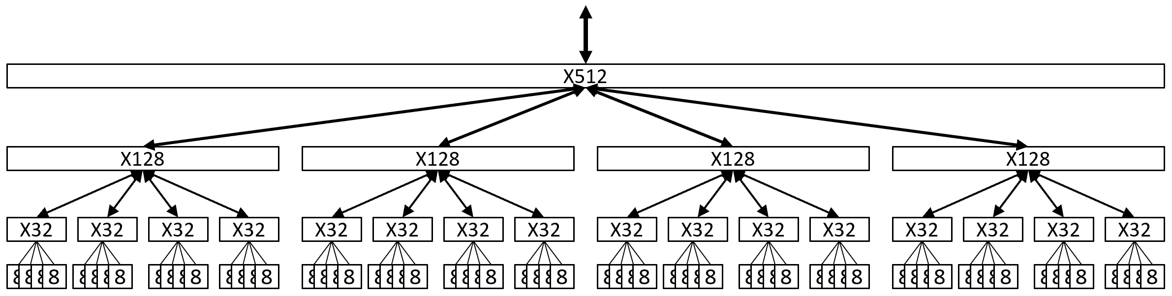
A hierarchical N=512 LUT quadrant of a large S3GA FPGA
At the leaves of this quadrant are sixty-four LB8s, each labeled 8. LB8s (hence LUTs) only appear at the leaves of the graph.
Each cluster of four LB8s is composed by an X32 switch. The X32 switch routes some subset of its 32 LUTs’ outputs up to its parent X128 switch, accepts some inputs from its X128 switch, and routes them down to its four LB8s as appropriate.
At the next level up, the X128 switch accepts subsets of LUT outputs from its four child X32 switches, as well as other input nets from its parent X512 switch, and routes input subsets of all these nets down to its four child X32 switches.
At the top level of this diagram, the X512 switch accepts subsets of LUT outputs from its four child X128 switches, as well as other inputs nets from its parent X2048 switch (not shown), and routes input subsets of all these nets down to its four child X128 switches.
With this architecture, global LUT placement is (mostly) finding the minimum cut 4-partition of the netlist hypergraph, and repeating min cut 4-partitions recursively until each subpartition fits in an LB8. A design “fits” into the device if its LUTs fit into the total LB8 capacity of the device, of course, and if the size of each cut is not greater than the capacity of the corresponding inter-switch bus. Following a successful hierarchical partitioning, routing requires scheduling which LUTs to evaluate in which cycles, and filling in so many input and output mux selection tables.
Reflecting Rent’s rule, the switch hierarchy need not “route up” every LUT output. For example, an LB8 might have 8 outputs to its parent switch, and the X32 switch might have 32 outputs, but the X128 switch might output only 64 of those 128, and the X512 switch might output only 128 of those 512.
Similarly, for input routing, an X128 switch might “route down” (different) 48 net subsets of its input nets for each of its four child X32 switches. (Specific switch I/O bus width parameters are TBD.)
Floorplan
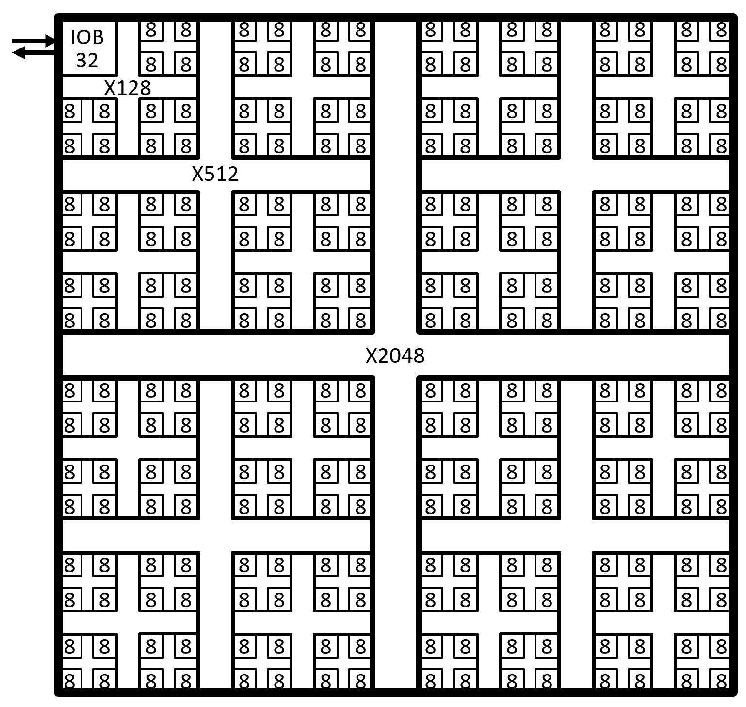
Here is an example floorplan for a N=2048 LUT S3GA device, reflecting the proposed recursive 2D 4-partitioning of the circuit. The first leaf cluster of four LB8s (32 LUTs) is replaced with a 32b IO block (“IOB32”).
Floorplan of a 2K LUT S3GA
Observe that a LUT output net from one LB8 to an adjacent LB8 at the same X32 switch need never leave that domain, whereas a LUT output in some X512 quadrant may be received as a LUT input in some other other X512 quadrant, by ascending an X32, X128, and X512 switch, up to the top-level X2048 switch, then descending an X512, X128, and X32 switch, down to the receiving LB8.
A serial interconnect fabric
S3GA’s LB8’s bit serial nature economizes standard cells per logical LUT. More significantly, it enables a remarkably frugal programmable interconnect fabric.
Referring to the older N=40 S4GA block diagram figure above, the five M=8 LUT clusters are passed by a bus of 64 nets (24 FPGA inputs and 40 LUT outputs). But each of these 40 LUT output wires changes only once per M=8 cycles. These 40 LUT outputs could be conveyed over five wires by serially streaming out LUT outputs into the interconnect fabric. Now the LUT input muxes that select input values from these LUT outputs can be just a (5-1):1 mux instead of a (40-8):1 mux. Now transmitting all 128 LUT outputs from a X128 switch quadrant requires only 16 wires (over 8 clock cycles). Now selecting one of these 128 outputs requires a 16:1 mux instead of a 128:1 mux (i.e., five mux4_1s cells instead of 42+ cells).
However serial transmission of LUT outputs on shared wires significantly complicates LUT cycle scheduling. If LUT A in some LB8 has an output net that is an input of LUT B in an adjacent LB8, it is necessary to schedule the LUT B evaluation one cycle after the LUT A, because that is the only clock cycle during which the A value is available on a LUT output wire. Use it or lose it! But if LUT B has a second input, LUT C, evaluated during a different clock cycle than LUT A, there is no clock cycle during which A’s and LUT C’s outputs are simultaneously available as LUT B inputs. Drat. We’ll address this problem momentarily.
So across the entire hierarchical interconnect fabric, S3GA conveys all LUT output nets in the M=8 serial time domain, eliminating (M-1)/M of all wires and their mux trees.
The serial interconnect fabric hierarchy
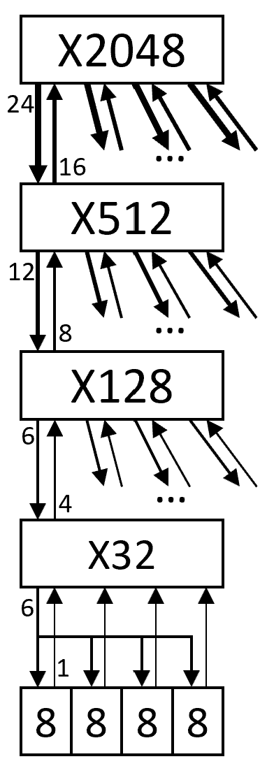
This figure revisits the N=512 LUT quadrant hierarchy figure above, labeling the switch input and output ports with strawman port widths, for one vertical slice of elements through the hierarchy. Remember these port widths are for bit serial ports, and convey, across eight clock cycles, eight times as many nets as port wires. For example, the four 16-wire ports that are the inputs of the top level X2048 switch, carry 4x16x8 = 512 output nets from the four X512 quadrants.
A slice through the switch hierarchy, labeled with serial interconnect I/O bus widths.
This table summarizes the strawman switch port width parameters.
Parameter
Value
Description
N
2048
no. of LUTs (incl. IOB32 as LUTs)
M
8
no. of logical LUTs per LUT (or, per logic block)
B
4
branching factor: no. of sub-clusters per cluster
O0
1
level 0: LB8: no. of serial outputs
O1
4
level 1: X32: no. of serial outputs
O2
8
level 2: X128: no. of serial outputs
O3
16
level 3: X512: no. of serial outputs
N4
64
level 4: X2048: no. of serial nets
I3
24
level 3: X512: no. of serial inputs
I2
12
level 2: X128: no. of serial inputs
I1
6
level 1: X32: no. of serial inputs
I0
9
level 0: LB8: no. of serial inputs
LB8 input deserialization
When a serial LUT output net is routed to and arrives at some LB8, it is selected as an LB8 input by one of I >=1 logic block input muxes, whether or not the net is an input for the logical LUT evaluation that cycle. This input net is buffered in one of I (M-deep) LB8 input buffers (serial-in parallel-out shift registers). This input net value may then be used as a LUT input during the next M LUT eval cycles of that LB8.
In the baseline (bit parallel interconnect) S4GA N=40 M=8 LUTs design, there are G=2 global inputs per LUT cluster, using two 40:1 muxes (each 13 mux4_1s). Adopting a bit serial interconnect and LB8 input deserialization, there are two 8:1 LB8 input muxes, two 8x1b LB8 input buffers, and two (8+8+…):1 LUT input muxes (5+… mux4_1s), each selecting a LUT input from the LB8 input buffers.
The base S4GA design requires M=8 x G=2 x clg(40) bits = 96b of configuration data to select two LUT inputs from the 40 bit parallel LUT outputs, whereas the bit serial version requires M=8 x I=2 x clg(5) bits = 48b of configuration data (LB8 inputs) plus M=8 x I=2 x clg(8+8+…) = 80b of config data for two LUT input selectors (LUT inputs). A 60% increase — worth it to mitigate LUT cycle scheduling constraints.
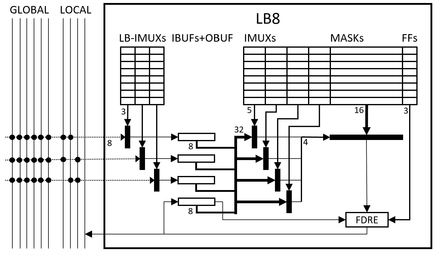
Level 0: M=8 logic block (LB8)
This figure shows the general structure of the M=8 I=3 K=4 logic block (“LB8”), now with block input muxes and buffers.
Architecture of LB8: M=8 I=3 K=4 LUT block
(Not shown: configuration logic, half-LUT cascade, D-FF clock enables and set/reset, and 32×8/64×4/128×2/256×1 true dual port RAM mode.)
At left, the block is passed by six global wires and four local wires. Global wires are serial input nets from afar, received via the block’s X32 switch. Local wires are the serial output nets of the four LB8s in this X32 cluster.
Each cycle the block inputs three of these nets, as selected by three 3b LB-IMUX selector fields. These three inputs are buffered in three 8b IBUF shift registers. Together these 24b plus the most recent 8 LUT outputs (the OBUF shift register) are the 32 possible input nets for the 4-LUT.
Next, four 5b IMUX selector fields select four of these 32 inputs as the 4-bit LUT input. This selects one of the 16 bits of the LUT mask as the LUT combinational output.
Then, the final output of the LUT net is determined by combinational output, the previous value of the LUT output (i.e., the M=8 shift-out bit of OBUF), the global reset input (not shown), the LB8 clock enable (CE) input (not shown), and the LUT’s 3b FF control field.
The new value of the LUT output net is captured in the OBUF shift register, and is output via a local wire to the other LB8s in this cluster, and to the X32 switch.
In an N=2048 LUT S3GA, 256 LB8s – 4 LB8s (IOB32) require about 252 x (8×48 + 32 + 4) = 252 x 420 = 105,840 configuration bits.
LB8 half-LUT cascade
Half-LUT cascade is a simple local optimization to implement adders efficiently. A n-bit ripple carry adder comprises a vector of n full adder cells. Each cell adds a[i], b[i], and carry[i-1], producing sum[i] and carry[i]. When this is technology mapped to a pure 4-LUT FPGA, it requires 2n LUTs for the 2n LUT outputs (sum[n-1:0] and carry[n-1:0]).
S3GA LB8’s provide half-LUT cascade to implement n-bit adders in n LUTs. S3GA provides a simple fracturable LUT, treating a k-LUT as two (k-1)-half-LUTs of the same k-1 inputs. So in addition to the usual full k-LUT output, which can be routed anywhere in the S3GA, an additional half-LUT (i.e., (k-1)-LUT) output, using the k-1 LSBs of the LUT input index, is also evaluated and registered in a “half_q” register for possible use as the half-LUT cascade-in in the next tick.
For example, when k=4, LUT inputs { 1’b1, half_q, b[i], a[i] } can index an adder LUT mask that produces sum[i] as the output of the full LUT (i.e., the upper half LUT) and carry[i] as the output of the lower half LUT. To select a half-LUT cascade input and half-LUT evaluation, a LUT’s k-1 and k-2 LUT input selectors are set to all-ones. The first special selector selects a constant 1; the second selects the current value of half_q.
To facilitate wide adders (up to n=32b in 32 LUTs / 4 LB8s), starting in any LB8, the half-LUT output of LUT #7 in each LB8 cascades into the half-LUT input of LUT #0 in the next LB8 in the four LB8-cluster. For those of you (properly) thinking serially, that means, in tick M-1=7, that the half-LUT output of each LB8 is registered as the next half-LUT input, for (pending) tick 0, in each next LB8 in the cycle (LB8 #0, #1, #2, #3, #0, …). Of course, unless adder sub-segments are pipelined, a ripple-carry 32b add still has a latency and an initiation interval of 32 ticks = 4 tocks.
TODO: illustrate half-LUT carry adders with a figure and LUT netlist.
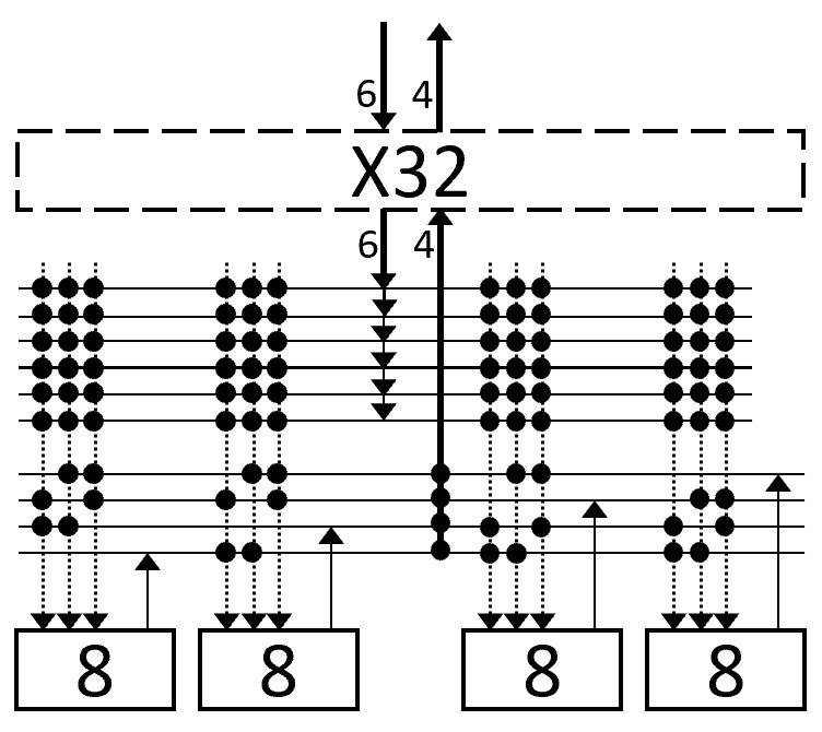
Level 1: Composing four LB8s with a (transparent) X32 switch
Four LB8s composed by a (transparent) X32 switch
In an N=2048 LUT S3GA, 64 X32s require zero configuration bits and zero muxes.
Level 1: IO block (IOB32)
The first (and only, for the time being) “X32 switch cluster” of four LB8s is replaced with an IOB32 block. This interfaces the serial interconnect S3GA with the greater parallel interconnect SoC. It consists of a configurable input crossbar selecting up to 32 inputs into a 4b serial output bus, plus a configurable output crossbar, receiving a 6b serial input bus and from that selecting and registering up to 48 parallel outputs.
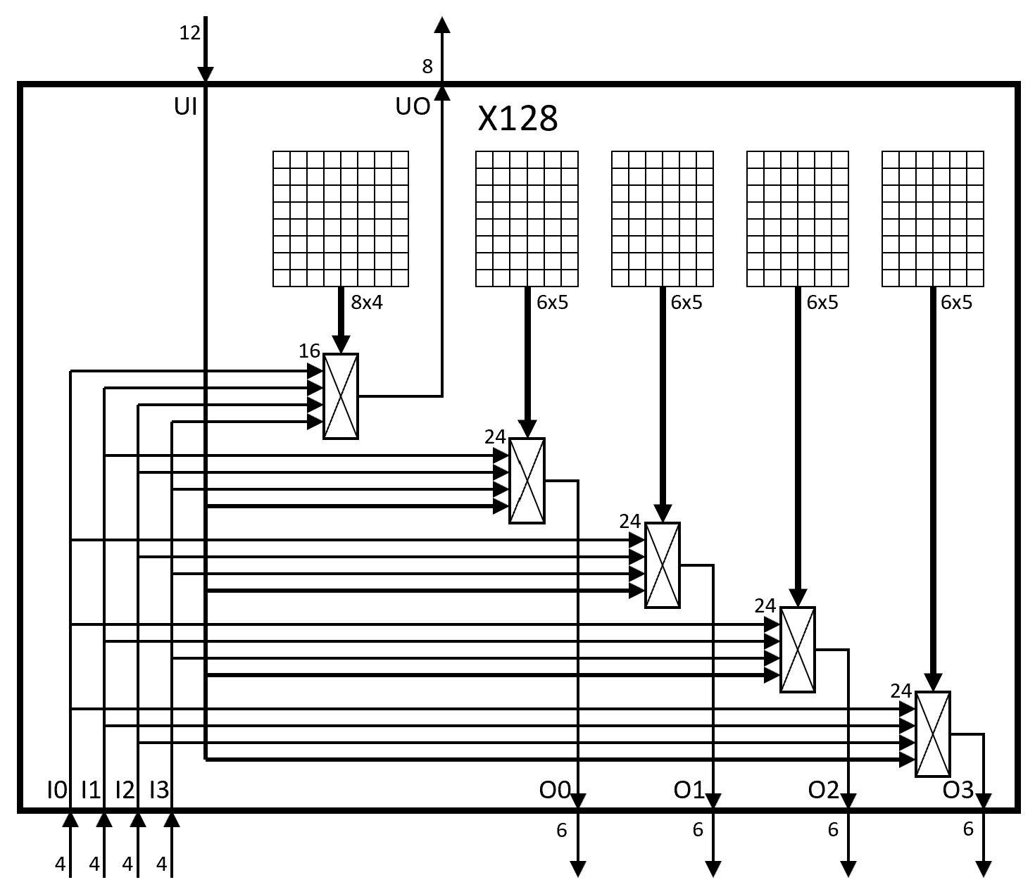
Level 2: Composing four X32s with an X128 switch
Architecture of an X128 switch
In an N=2048 LUT S3GA, sixteen X128s require 16 x (8x8x4 + 4x8x6x5) = 16 x 1,216 = 19,456 configuration bits and 16 x (8×16:1 + 4x6x24:1) muxes = 16 x (8×5 + 24×8) mux4_1s = 16 x 232 mux4_1s = 3,712 mux4_1s.
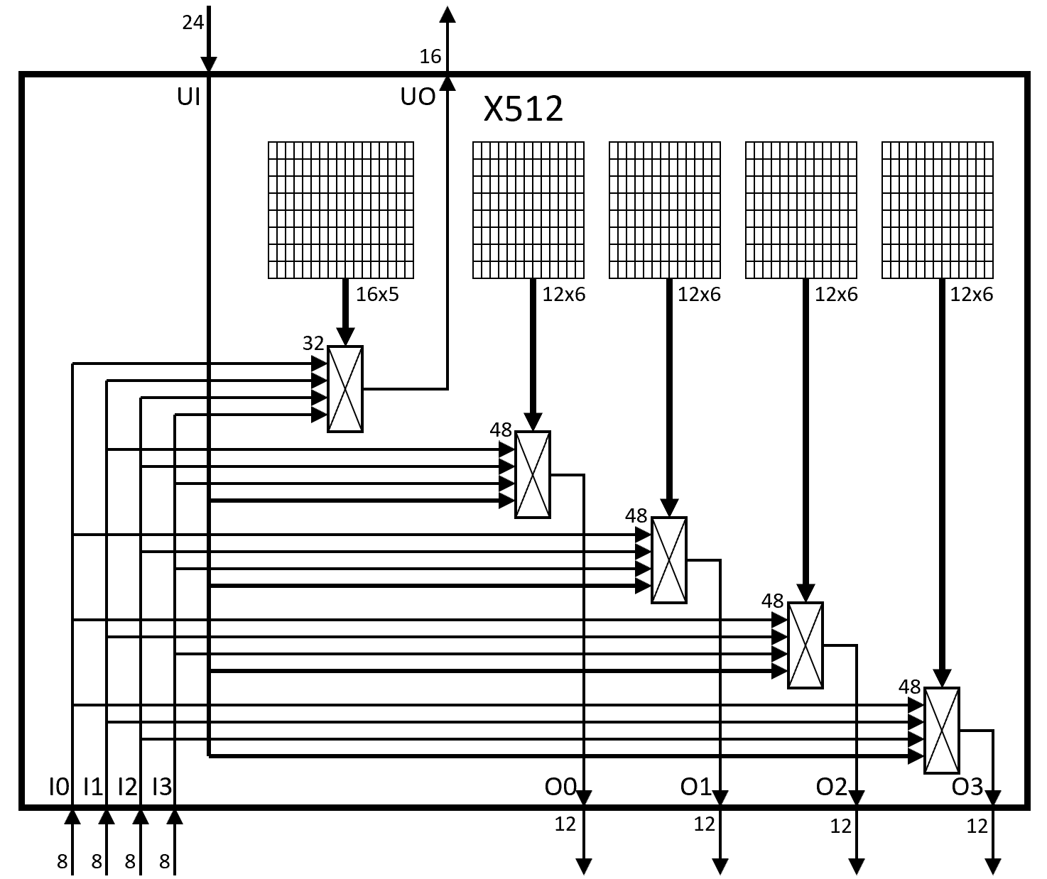
Level 3: Composing four X128s with a X512 switch
Architecture of an X512 switch
In an N=2048 LUT S3GA, four X512s require 4x (8x16x5 + 4x8x12x6) = 4 x 2,944 = 11,776 configuration bits and 4 x (16×32:1 + 4x12x48:1) muxes = 4 x (16×11 + 48×16) mux4_1s = 4 x 944 mux4_1s = 3,776 mux4_1s.
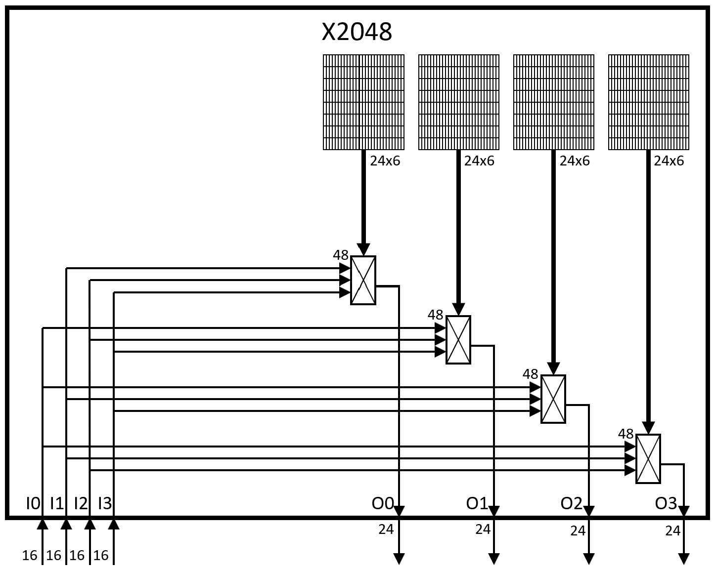
Level 4: Composing four X512s with a X2048 switch
Architecture of an X2048 switch
In an N=2048 LUT S3GA, one X2048 requires 4x8x24x6 = 4,608 configuration bits and 4x24x48:1muxes = 96×16 mux4_1s = 1,536 mux4_1s.