“An FPGA is just a clever heap of multiplexers and mux select memory”
S3GA RTL v1 is now available on our S3GA github repo.
A 2000 LUT configuration, implemented with Openlane
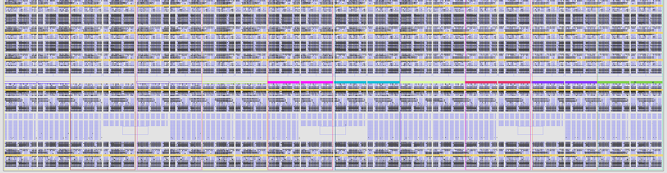
Here is the first implementation of the S3GA<N=2048,M=8,K=4> design, which fits in the efabless Open Shuttle Program‘s ~10mm2 caravel_user_project area (2.92mm x 3.52mm) for the 130nm Skywater PDK, as produced by the wonderful OpenLane tools.
Implementation plus signoff checks take about 7 hours. At peak the tools used 60 GB of RAM. There are 2 wee Magic design rule check failures to investigate. Some design stats: 141,000 DFFs, 14,000 mux4s and 19,000 mux2s. This first cut has a 9 ns clock period = M=8-cycles at 72 ns = 14 MHz.
Next: DFFRAM?
This design uses 256-4=252 eight 4-LUT logic blocks (LB8s) (see part one), each of which uses an 8x48b configuration memory — an 8-entry x 48b circular shift register.
I hope to replace the hundreds of 8x configuration memories with bespoke, placed (floorplanned) instances of DFFRAM macros. This should also make it more practical to add a LUT-RAM mode to LB8s, so they may also be used as true dual port 32×8 SRAMs and possibly as 2R1W-64×4 SRAMs. Thus each X32 tile could implement a 32×32 register file.
It should also be possible to replace some X128 tiles with 100% DFFRAM or OpenRAM based block RAM (BRAM) cells at >3x the density of S3GA LUT-RAM.
Onwards!