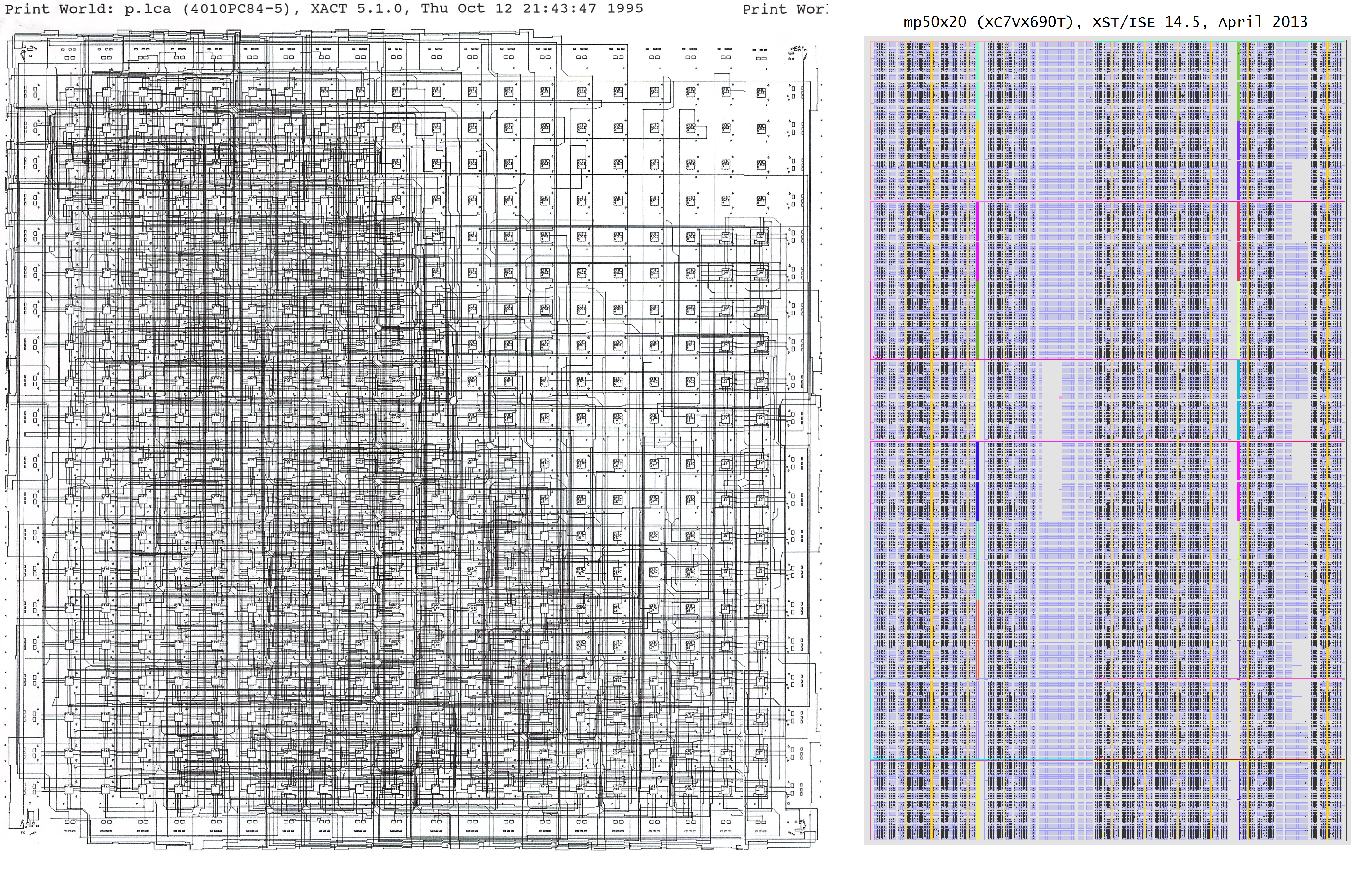
On the left, from 1995, J32, one 32-bit RISC SoC in an XC4010. It had 20x20x2=800 4-LUTs (and 400 3-LUTs).
On the right, from 2013, 1000 32-bit RISC datapaths and 250 router cores in an XC7VX690T (which provides over 433,000 6-LUTs and 1470 BRAMs). A work in progress.
In other words, in the past 18 years Moore’s Law has taken us from 1K LUTs per FPGA to 1K 32-bit CPUs per FPGA.


Hi Jangray,
Along the same lines,, How should I approach designing a USB interface for a FPGA? What are the options I have?
Cheerio
Very interesting! By coincidence, I was recently pondering what an optimal chip for my Cuckoo Cycle proof-of-work algorithm could look like (http://www.reddit.com/r/dogecoin/comments/210y4a/how_to_stop_asics_and_multipools_xpost_github/cg8qnge) and it was surprisingly similar to your FPGA design. So now I’m curious, can your design be adapted to supporting external DRAM? Can you interface to DIMMs, accessing single 32-bit words at a time, rather than entire cache lines? And if so, how many cpus could simultaneously make random memory accesses before the DRAM is saturated?