Tag Archives: Phalanx

GRVI Phalanx at Hot Chips 29 (2017)

Yesterday at Hot Chips 29 (2017) I presented a poster GRVI Phalanx: A Massively Parallel RISC-V FPGA Accelerator Framework: A 1680-core, 26 MB SRAM Parallel Processor Overlay on Xilinx UltraScale+ VU9P (PDF) and some hardware demos. Extended abstract (PDF). 
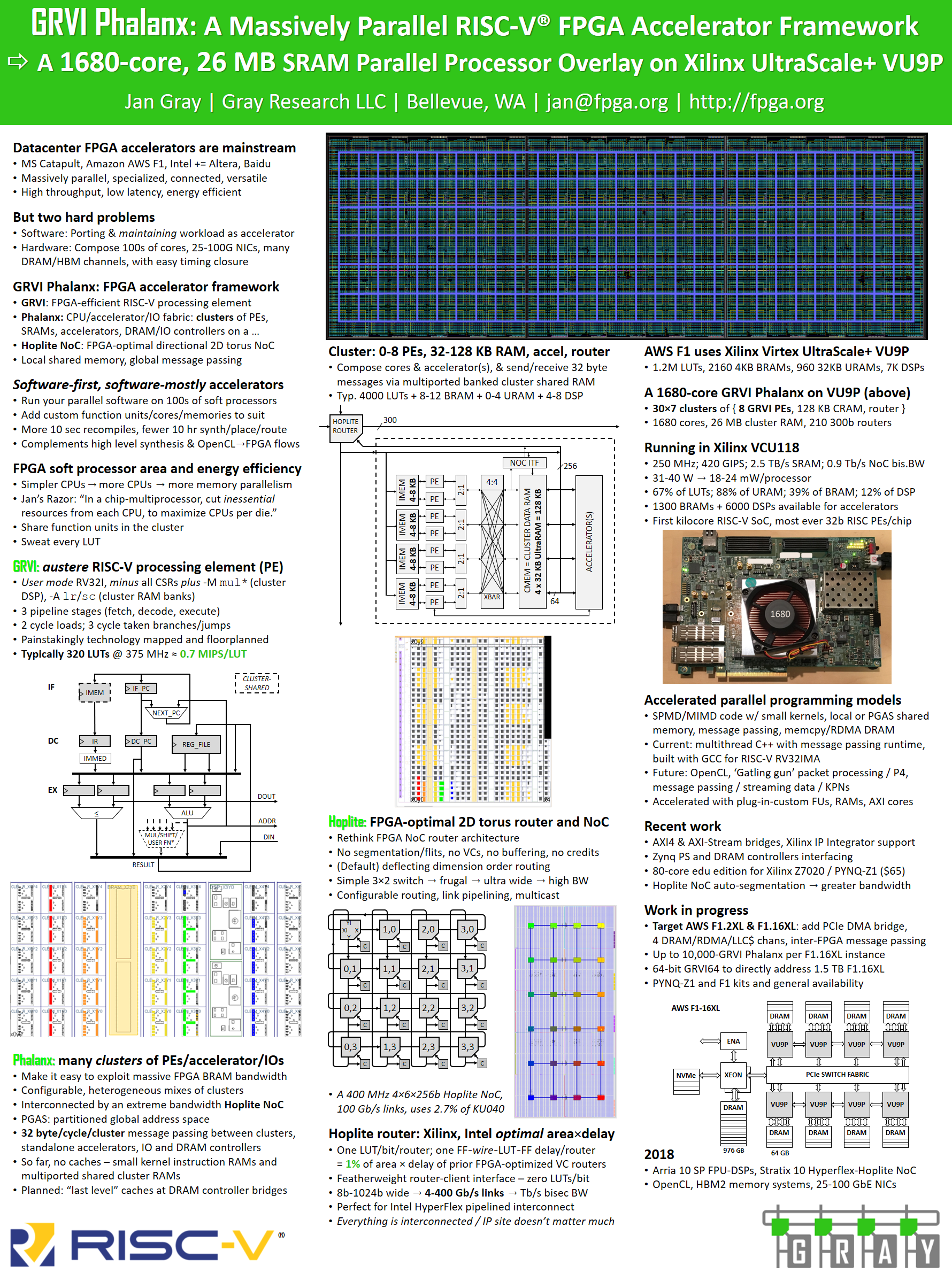
The poster focuses on the Dec. 2016 1680 core milestone but also describes plans and ideas for programming models and tools, and recent work towards AWS F1 and PYNQ-Z1 general availability, including work on AXI4-MM and AXI4-Stream bridges to the Hoplite NoC fabric, enabling AXI4 DRAM / Phalanx-RDMA interface support for Zynq 7000 (hard DRAM controllers behind the HP[0-3] ports) and AXI4 64b DDR4-2400 MIG DRAM interfaces on KU040 and VU9P.

In the adjacent RISC-V Foundation booth, I set up two demos:

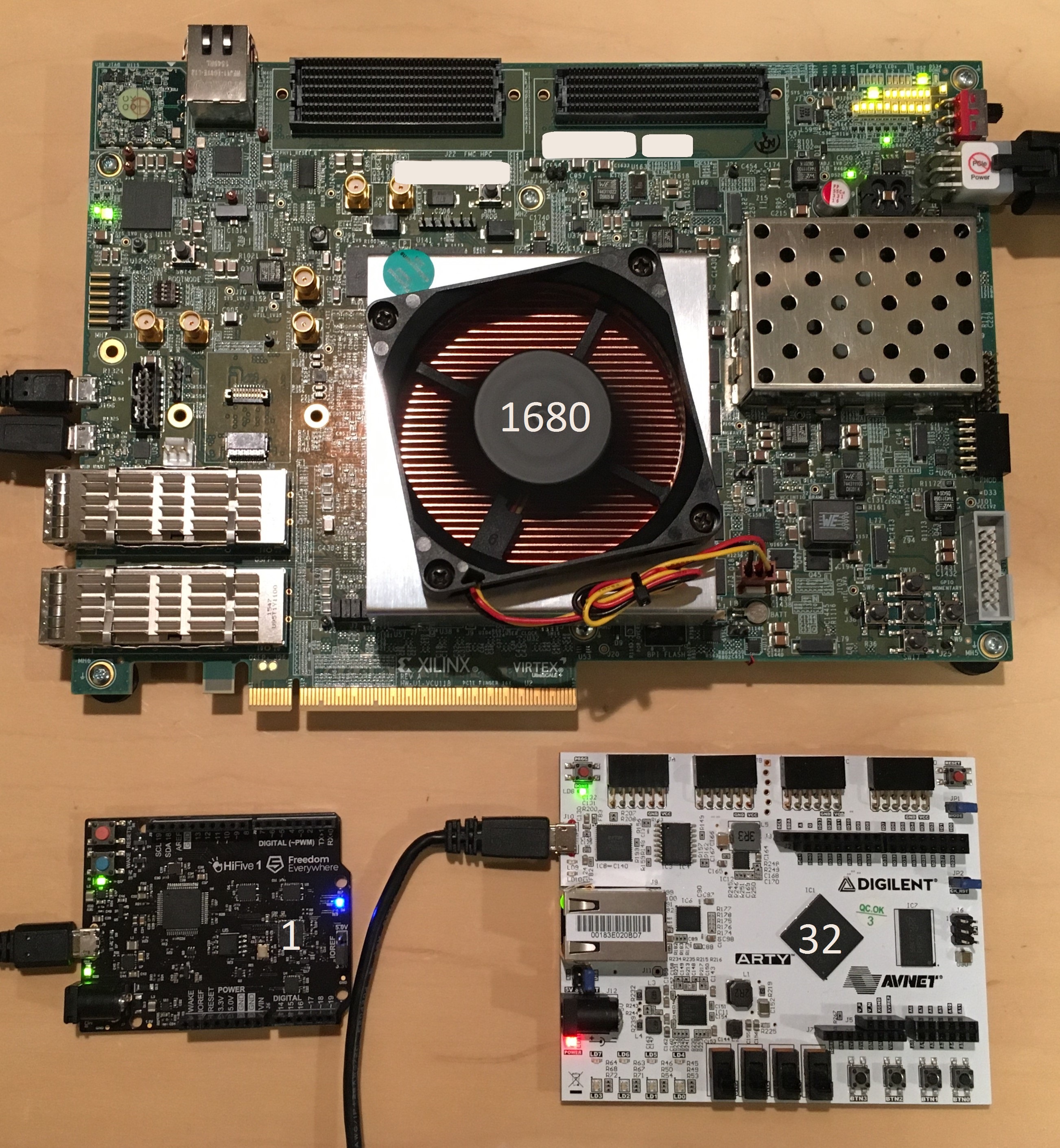
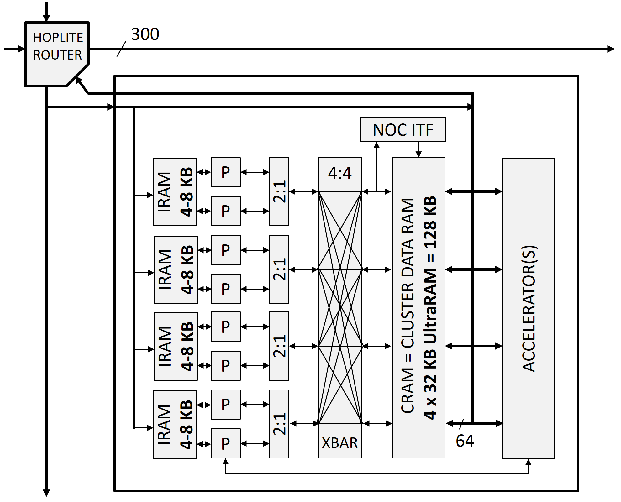
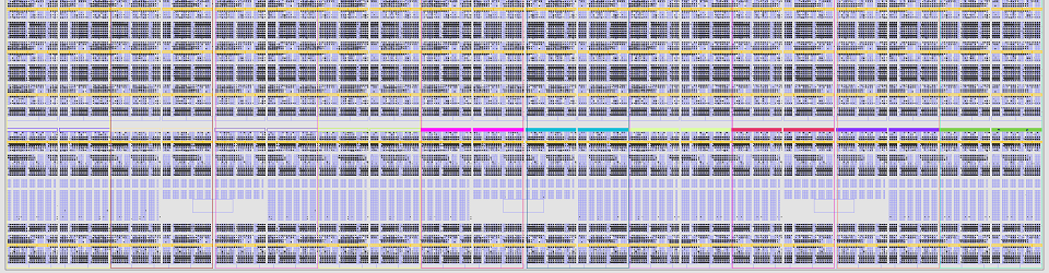
  • A 1680-core, 26 MB GRVI Phalanx on VU9P on VCU118, with a 7×30×300b Hoplite NoC and 7×30 clusters of { 8 RISC-V cores + 128 KB }, running a message passing, bulk synchronous integer matrix multiplies demo, and
  • An 80-core GRVI Phalanx on 7Z020 on PYNQ-Z1, with a 4×4×300b Hoplite NoC and 10 clusters of { 8 RISC-V cores + 32 KB }, running an AXI4 DRAM/RDMA bridge test of 80×256B×2^28 reads. (Some of the 80 cores’ blue and white subwindows of the console are visible in the photo below.)

This just underscores that I need to invest in better demos.

Photo of demos of GRVI Phalanx on PYNQ-Z1 (80 cores) and VCU118 (1680 cores) at the RISC-V table at Hot Chips 29

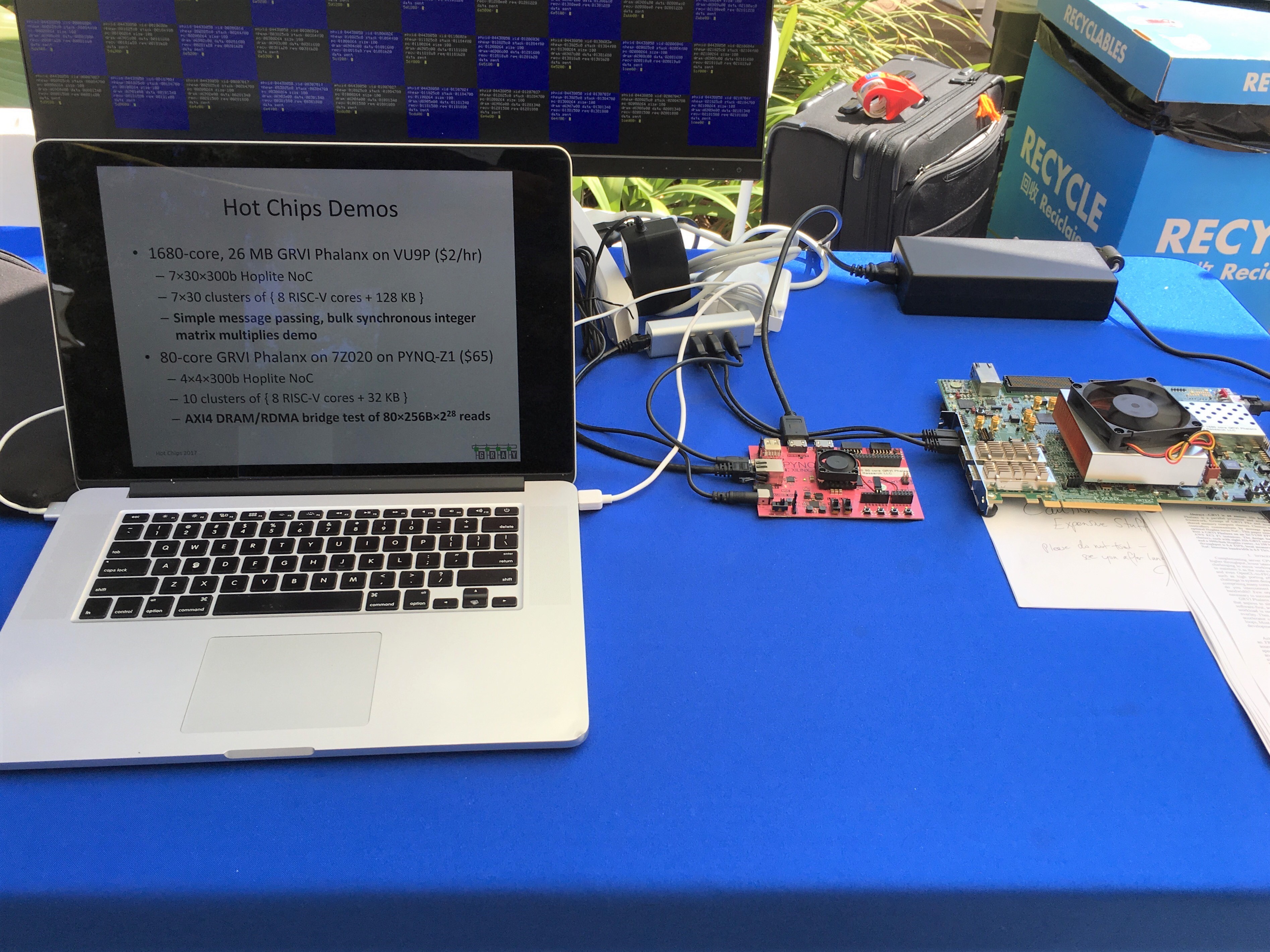
Demos of GRVI Phalanx on PYNQ-Z1 (80 cores) and VCU118 (1680 cores) at the RISC-V table at Hot Chips 29

This event was a special occasion for me. I’ve attended Hot Chips conferences since the late 1980s. Then, as a software engineer fascinated by computer architecture and following USENET’s comp.arch gang, it was a thrill for me to head to Stanford and meet my heroes, microprocessor architects, and learn more about how their new parts worked, and I’d return with new insights that made me a better software engineer.

Back in the ’80s, only chip design teams had the EDA tools and fabs necessary to build microprocessors. But starting in the ’90s, larger and more capable FPGAs, with increasingly comprehensive tools and infrastructure, enabled anyone to develop FPGA CPUs and now parallel computers. FPGAs democratize access to high performance digital design, and yesterday to bring this full circle, I demonstrated a parallel computer system on a chip integrating the greatest number of 32-bit RISC processors ever. With this kind of work, and with the Microsoft Brainwave announcement, FPGA designers are emphatically not second class, second best to inflexible ASICs. Rather FPGA platforms are coequal and indeed are the vanguard of agile computer architecture.

GRVI Phalanx joins The Kilocore Club

The work-in-progress GRVI Phalanx massively parallel accelerator framework has been ported to the Xilinx Virtex UltraScale+ XCVU9P.

On Dec. 30, 2016, a design with 30 rows by 7 columns of clusters of 8 GRVI RISC-V cores + 128 KB CRAM (cluster RAM) + a 300-bit Hoplite NOC router — a total of 1680 cores and 26 MB of SRAM — booted up and tested successfully, running a message passing matrix multiply workload on all 1680 cores, in a XCVU9P-FLGA2104-2L-E-ES1 device in a Xilinx VCU118 evaluation kit.

This 1680 core GRVI Phalanx is the first operational kilocore RISC-V, the first kilocore 32b RISC in an FPGA, and the most 32b RISC cores on a chip in any technology.

1 core, 32 cores, 1680 cores -- RISC-V scales up! A 1-core Si-Five HiFive-1, a 2x2x8=32-core GRVI Phalanx in a Digilent Arty / XC7A35T, and a 30x7x8=1680-core GRVI Phalanx in a Xilinx VCU118 / XCVU9P

1 core, 32 cores, 1680 cores — RISC-V scales up! A 1-core Si-Five HiFive-1, a 2x2x8=32-core GRVI Phalanx in a Digilent Arty / XC7A35T, and a 30x7x8=1680-core GRVI Phalanx in a Xilinx VCU118 / XCVU9P.

Here is the basic cluster tile architecture redesigned for UltraScale+ and its new 288 Kb UltraRAM jumbo-SRAM blocks. The present design includes 210 instances of this tile.

A GRVI Cluster tile with 8 GRVI RISC-V cores, 128 KB multiported bank interleaved shared cluster RAM, optional accelerators (here, none), and a 300-bit wide Hoplite NOC router.

A GRVI cluster tile with 8 GRVI RISC-V cores, 128 KB multiported bank interleaved shared cluster RAM, optional accelerators (here, none), message passing NOC interface, and a 300-bit wide Hoplite NOC router.

An example 1680 GRVI system implemented in a Xilinx Virtex UltraScale+ VU9P. This GRVI Phalanx comprises NX=7 x NY=30 = 210 clusters, each cluster with 8 GRVI cores and a 8-ported 128 KB cluster shared memory. The clusters are interconnected on a Hoplite NOC, with the Hoplite routers configured with 290b data payloads (including 32b address and 256b data), achieving a bandwidth of about 70 Gb/s/link and a NOC bisection bandwidth of 900 Gb/s. Each cluster can send or receive 32 B per cycle into the NOC. The GRVI Phalanx architecture anticipates a variety of configurable accelerators coupled to the processors, the cluster shared RAM, or the NOC.

An example 1680 GRVI system implemented in a Xilinx Virtex UltraScale+ VU9P. This GRVI Phalanx comprises NX=7 x NY=30 = 210 clusters, each cluster with 8 GRVI cores and a 8-ported 128 KB cluster shared memory. The clusters are interconnected on a Hoplite NOC, with the Hoplite routers configured with 290b data payloads (including 32b address and 256b data), achieving a bandwidth of about 70 Gb/s/link and a NOC bisection bandwidth of 900 Gb/s. Each cluster can send or receive 32 B per cycle into the NOC. The GRVI Phalanx architecture anticipates a variety of configurable accelerators coupled to the processors, the cluster shared RAM, or the NOC.

An extended abstract with additional detail on this work has been submitted to, and hopefully will be presented at, the OLAF’17 workshop at FPGA’17.

GRVI Phalanx Update

An update on the work-in-progress GRVI Phalanx.

Conferences

An extended abstract and brief talk on GRVI Phalanx was presented at the 2nd International Workshop on Overlay Architectures (OLAF-2) at FPGA 2016.

GRVI Phalanx was discussed in the short talk Software-First, Software Mostly: Fast Starting with Parallel Programming for Processor Array Overlays at the Arduino-like Fast-Start for FPGAs pre-conference workshop at FCCM 2016. [Slides]

The first refereed paper on GRVI Phalanx was presented yesterday at the 24th IEEE International Symposium on Field-Programmable Custom Computing Machines (FCCM 2016): GRVI Phalanx: A Massively Parallel RISC-V FPGA Accelerator Accelerator and received the FCCM 2016 Best Short Paper Award. [PDF]

Hardware Changes: Version 0.2

Here are some of the changes made to the GRVI Phalanx design since it was first described at the 3rd RISC-V Workshop. This is now version 0.2.

GRVI

  • LB/LBU/LH/LHU/SB/SH: Load/store byte and halfword alignment functionality is now configured OFF in the GRVI PEs. The LdMux and StMux units have been factored out of GRVI and into the GRVI cluster, each set of muxes shared by a pair of cores.
  • MUL/MULH/MULHU/MULHSU: The multiply instructions from the RISC-V “M” extension are now enabled by default and are implemented in the GRVI cluster. Each pair of processors shares one DSP-based multiplier. This consumes 200 DSP48s in the 400 PE GRVI Phalanx for Kintex UltraScale 040, leaving 1720 DSP48s for use by accelerators.
  • SL*/SR*: By default, fast left and right shift instructions are also implemented in these DSP-based multipliers.
  • LR/SC: These atomic instructions from the RISC-V “A” extension are now enabled by default. Part of the implementation is in the GRVI core and part in the GRVI cluster memory arbiters. The implementation considerations were discussed on the RISC-V mailing lists here.

Phalanx

  • A Phalanx system may be configured to replace the cluster at (NX-1,NY-1) with a character mode VGA cluster with a 32 KB text frame buffer.
  • Hoplite multicast message routing is now enabled by default. An agent can sent a message to every cluster on a given row, given column, or to every cluster on the NOC. If desired, all IRAMs in all clusters in a Phalanx may be updated with a single burst of 1024 XY-multicast messages.

Introducing GRVI Phalanx: A Massively Parallel RISC-V FPGA Accelerator Accelerator

GRVI is an FPGA-efficient RISC-V RV32I soft processor core, hand technology mapped and floorplanned for best performance/area as a processing element (PE) in a parallel processor. GRVI implements a 2 or 3 stage single issue pipeline, typically consumes 320 6-LUTS in a Xilinx UltraScale FPGA, and currently runs at 300-375 MHz in a Kintex UltraScale (-2) in a standalone configuration with most favorable placement of local BRAMs.

Phalanx is massively parallel FPGA accelerator framework, designed to reduce the effort and cost of developing and maintaining FPGA accelerators. A Phalanx is a composition of many clusters of soft processors and accelerator cores with extreme bandwidth memory and I/O interfaces on a Hoplite NOC.

GRVI Phalanx was introduced today at the 3rd RISC-V Workshop at Redwood Shores, CA.

A work-in-progress 5x10x8 = 400 processor configuration in a KU040 in a Xilinx KCU105 and a 2x2x8 = 32 processor configuration in a Xilinx Artix-7 35T in an Digilent Arty were demonstrated in the demo/poster session.

A 10x5x8 = 400 processor GRVI Phalanx

For more information please visit the GRVI Phalanx page.