In this post we review the design and history of MX format reduced precision block floating point vector data formats. In the next post, we explore several possible RISC-V composable custom extensions to compute over them.
Microsoft team demonstrates a more frugal way to do AI tensor math, rivals unite in support
This MX Alliance proposes standards for new 4b, 6b, 8b floating point element and 8b integer element block floating point formats that are poised to obsolete use of 16-bit and wider floating point formats within matrix multiplies and convolutions in machine learning training and inference workloads.
A block floating point format replaces the k exponent terms of the individual elements of a block of k elements with a single common scaling term, X, stored once. All elements’ mantissas are scaled for that X term. This significantly reduces the block’s memory footprint, and dramatically reduces the logic resources (ASIC gates or FPGA LUTs) required to implement vector operators (esp. vector dot product). The Spec:
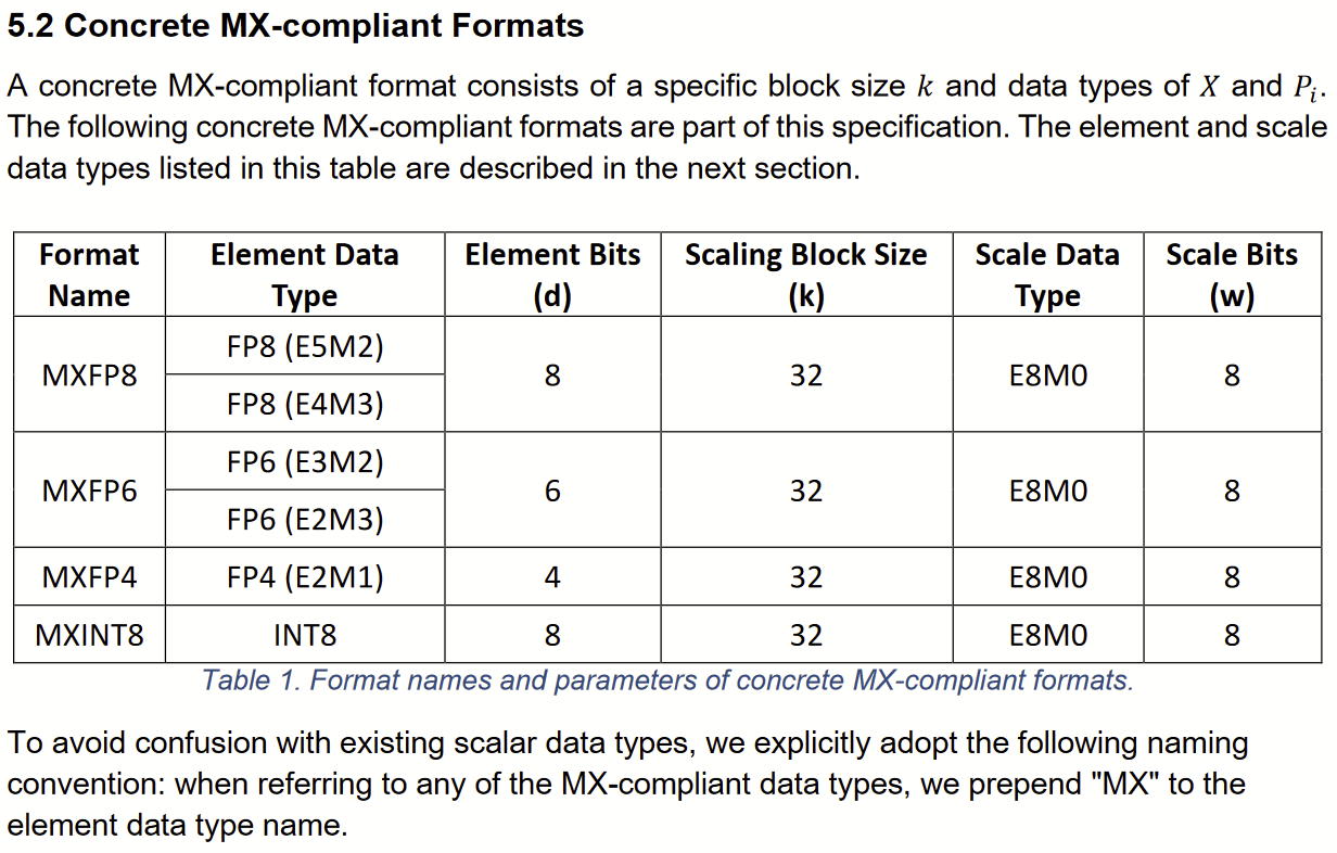
For MX formats, blocks have k=32 elements, the scale factor X is an 8b exponent, and elements may be FP4, FP6, FP8, or INT8:
Thus a 32 element MXFP6 block requires 32×6b element data + 8b scale data = 200 bits, and a 256 element vector, in memory, might use 8 MXFP6s = 200 bytes (or more!).
The accompanying whitepaper Microscaling Data Formats for Deep Learning, evaluating various MX formats on real ML workloads, justifies the interest and expected uptake of these formats. For example, the paper finds “MXFP6 closely matches FP32 for inference after quantization-aware fine tuning” and “generative language models can be trained with MXFP4 weights and MXFP6 activations and gradients incurring only a minor penalty in the model loss.”
For these AI tensor math workloads, MX format data achieves comparable accuracy using only a small fraction of the circuit resources of FP32 data.
A curiously unspecific specification
The spec declines to specify such essentials as: 1) a canonical in-memory representation of MX data; 2) the required internal precision and final precision of MX dot product; and 3) besides element-wise conversion to/from float32, and dot product, what other MX operations are required, and at what internal and final precision? For example:
5.1 Microscaling (MX): “The layout of the block in physical memory is not prescribed in this specification.”
6.1 Dot Product of Two MX-compliant Format Vectors: “The dot product of two MX-compliant format vectors of length k is a scalar number C. … The internal precision of the dot product and order of operations is implementation defined.”
Also, per 6.2 General Dot Product, the dot product of two arbitrary vectors is the sum of the dot products of their constituent MX k-vectors, with type float32. Here again the specification does not prescribe the type, precision, or order of evaluation of the intermediate sums terms (if any).
Leaving these details unspecified is problematic. Diverse “compliant” MX libraries and cores will evaluate the same models but with different results. Perhaps these omissions are intentional, and necessary to secure endorsements from rivals with quite different means of evaluating MX dot products.
George Constantinides (Imperial College) also writes about this here: Industry Coheres around MX? “To my mind, the problem with this definition is that × (on elements), the (elided) product on scalings and the sum on element products is undefined. …”
Paper trail
Now let’s review prior work that (I believe) led these researchers to these new data formats.
Project Catapult at ISCA 2014
Project Catapult. Putnam et al, A Reconfigurable Fabric for Accelerating Large-Scale Datacenter Services, ISCA 2014. DOI. PR. This well cited paper documents Microsoft’s early Project Catapult work to use parallel FPGA overlay architectures, across myriad FPGAs, to accelerate Bing query document ranking at scale. “We describe a medium-scale deployment of this fabric on a bed of 1,632 servers, and measure its efficacy in accelerating the Bing web search engine.” (I built the §4.6. Document Scoring gadget stage of this ranking pipeline; working with the MSR and Bing teams was a career highlight.) I believe Catapult spurred Intel to acquire Altera for $17B in 2015.
Project Catapult’s investments in people and in datacenter-networked FPGAs hosting hardware microservices planted the seeds of Project Brainwave.
Project Brainwave at Hot Chips 2017
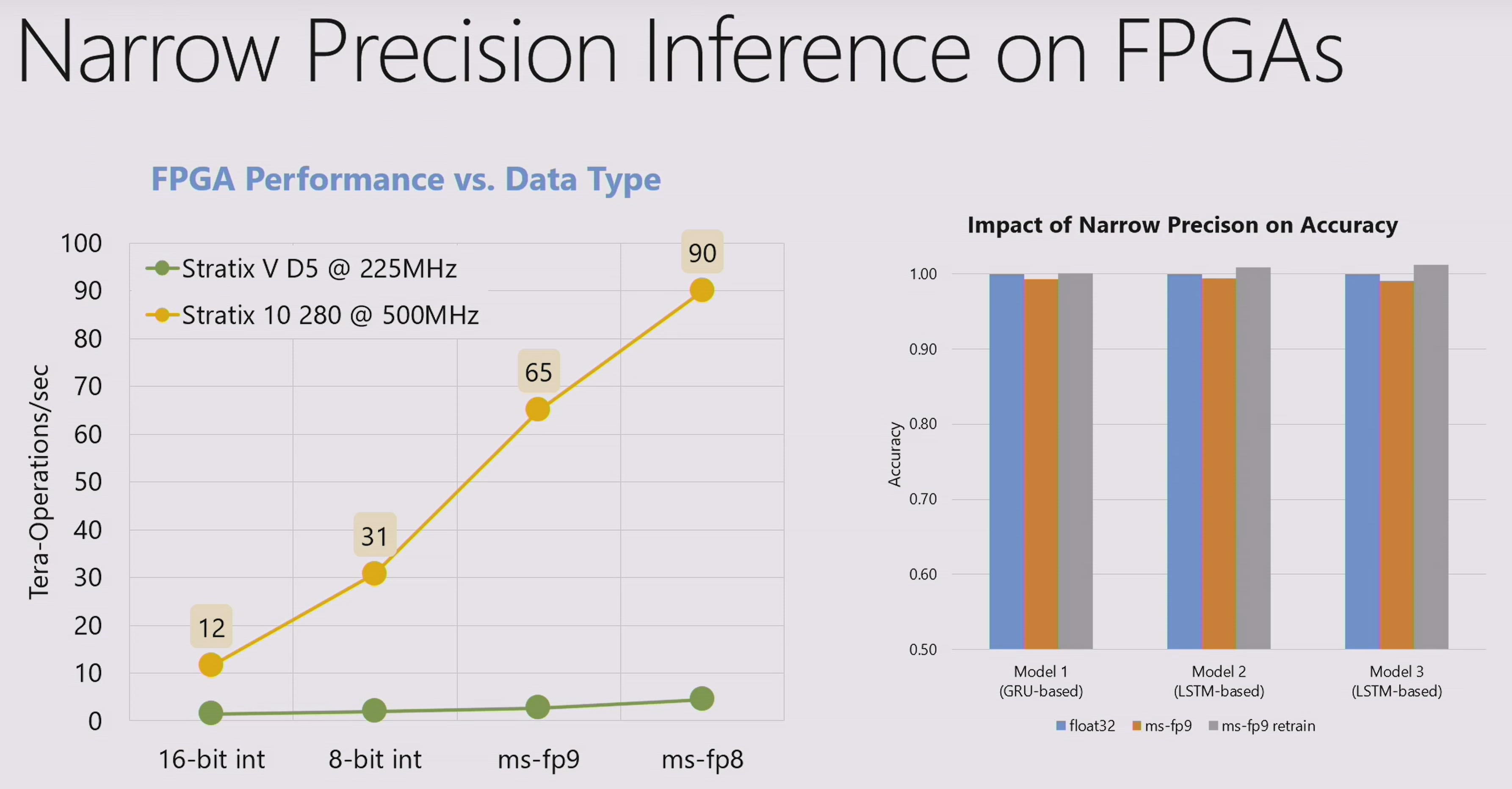
Project Brainwave. Chung and Fowers, Accelerating Persistent Neural Networks at Datacenter Scale, Hot Chips 2017. Video. The public debut of Brainwave. Leveraging FPGA hardware microservices at massive scale, it achieves high throughput, peak hardware utilization, and very low latency for batch size = 1 workloads, by keeping then-enormous ML models, many millions of parameters, entirely in SRAM across thousands of FPGAs’ × thousands of BRAMs, using tens of TBs/s/FPGA of SRAM bandwidth.
Fowers detailed the Brainwave soft DPU microarchitecture, including thousands of dot product units, totaling ~96,000 FMACs using narrow precision MS-FP floating point format: 90 TOPS ms-fp8 at 720 GFLOPS/W on Stratix 10 280. Despite quantization, its inference accuracy was comparable to float32 (after some retraining).
Brainwave’s mysteriously good floating point throughput
At the time I wondered, “How did Microsoft hit 90 TOPS? The no. of Stratix 10 DSPs × DSP Fmax << 90 TOPS. So some/most Brainwave FPUs must be in soft logic (LUTs). But 90 TOPS?! How?” To reproduce their result, I carefully designed frugal 8b and 6b FPUs, for Virtex UltraScale+ FPGAs. Try as I might, I couldn’t get to 90 TOPS. I wrote in 2017:
#FPGA noodling on LUT-frugal reduced precision floating point. fp8 = fp8*fp8 fp8 = fp8+fp8 fix16 += fp8*fp8 // commutative sum Thinking { sign:1; exp:4; mant:3 } per Deep CNN Inference with Floating-point Weights and Fixed-point Activations, flush-to-zero. For fp8 ::= { s:1; e:4; m:3 }, fp11 ::= { s:1; e:4; m:6 }: fix16 += (fp8)(fp8*fp8); // ~38 LUTs fix16 += (fp11)(fp8*fp8); // ~46 LUTs Pipelined at 500 MHz, in 1.2 M LUT XCVU9P * 90% utilization => ~28000 instances of fix16 += (fp8)(fp8*fp8) => 28 TFLOPs. (20+ TFLOPS in F1?) Eats 2*28K=56 KB/cycle. In a VU9P: 2160 BRAMs * 8 B/BRAM = 17KB/cycle; 960 URAMs * 16 B/URAM = 15KB/cycle. So requires weight or activation reuse. (Compare with XNOR-Net: 36b dot product = 50 LUTs per FPGA Hacks: Population count; VU9P URAM+BRAM bandwidth: 294Kb/cycle => ~300 TOPS @500 MHz with operand reuse.) For fp6 ::= { s:1; e:3; m:2 }, fp8x ::= { s:1, e:3; m:4 }: fix10 += (fp6)(fp6*fp6); // ~21 LUTs fix10 += (fp8x)(fp6*fp6); // ~24 LUTs Pipelined at 500 MHz, in 1.2 M LUT VU9P * 90% util => ~51000 instances of fix10 += (fp6)(fp6*fp6) => 51 TFLOPs. (40 TFLOPS on F1?) Even fp6 doesn’t match Brainwave’s “90 TFLOPs ms-fp8” on 500 MHz Stratix-10. Perhaps they are not using fused fp-mul-accumulate?
Multiplying is easy, young man, adding is harder
Where do the LUTs go in reduced precision FPGA FMACs?
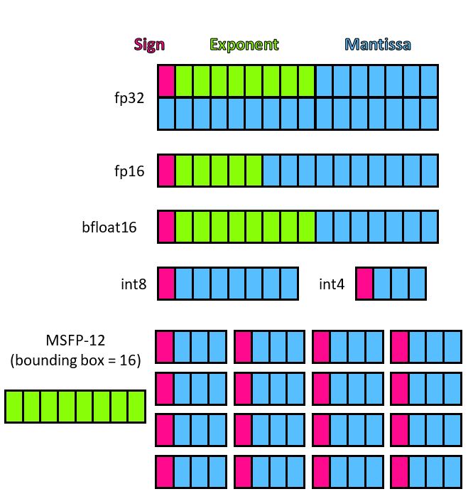
First let’s adopt the MX Spec notation: “ExMy: Notation for a scalar format with one sign bit, x exponent bits, and y mantissa bits. E.g., E4M3 refers to an FP8 format with one sign bit, four exponent bits, and three mantissa bits.” (Mantissa bits is a misnomer here; these are fraction bits (after the binary point), not including the implicit leading 1., or 0. when the number is a denormal.) So working in E4M3 { s:1; e:4; f:3; }, that’s a 1b sign, 4b exponent, and 3b fraction(i.e., a 4b significand with an implied leading 1). It exactly represents certain real numbers such as 240.0 (+1.1112 x 27) and -1.02 x 2-7 = -.0078125.
It is inexpensive to multiply such low precision floats in 6-LUT FPGAs. For example assume (flush-to-zero) normalized E4M3 × E4M3 products have a target precision of E4M6. The product of two E4M3 1.f 4b significands lie in [1.0000002 , 11.1000012]. If the product >= 2.0, normalize it by shifting the binary point to the left, i.e., 1.11000012 x 2-1, and round/truncate the (underlined) least significant bit. Then multiplication is just a table lookup of the resulting 6b fraction after normalization and rounding. With 3b fraction inputs a.f and b.f you require 23+3 = 64 entries, perfect for a 6 6-LUT 64x6b ROM. Add one LUT for the (>=2.0) shift signal and 0.5 of a 5,5-LUT for the XOR of the sign bit. Add 0.5-2 LUTs for zeroes. The (twice biased) product exponent is (a.e + b.e + shift), 4 LUTs. In all, perhaps 14 LUTs and two LUT delays. Cheap.
The greater cost of the dot product’s multiply-accumulate is the adder / adder tree. The sum of (e.g.) four element-wise products 1×2-6 + 1×2-4 + 1×2-2 + 1×20 = 1.0101012 x 20. Naively each add requires a pre-addition shifter to align mantissas, an add/sub, and then a CLZ circuit and another shifter to renormalize the sum/difference. How wide those shifters are, how wide the sum reduction adder precision is, ideally, depends on the adder tree requirements. But compared to the two LUT delays of of the multiplier, this FP reduction adds more LUT delays / pipeline stages as well as area. “It all adds up.”
My 2017 preference was and is to keep the vector reduction sum in fixed point and first convert each product mantissa term to fixed point with a barrel shifter, the shift count controlled by the product term’s exponent. Then reduction order doesn’t matter — fixed point adds are commutative. When I tried this in 2017:
So the above ~14 LUT multiply incurs an additional ~16 LUT shift and ~16 LUT add/sub. Roughly 2/3 of the FMAC is the adder. Ouch. How does that translate into TOPS? For an XCVU9P device, 1.2 MLUTs × 0.9 / 38 LUTs/mulacc = ~28000 mulaccs × 2 ops/clock × 0.5 GHz = 28 TOPS.
I tried again with 6b×6b floating point but that only reached ~50 TOPS.
About half of Microsoft’s 90 TOPS result, in a comparable one million 6-LUT device. I was stumped.
Then came: Chung et al, Serving DNNs in Real Time at Datacenter Scale with Project Brainwave, IEEE Micro, March 2018. DOI. The Hot Chips follow-on IEEE Micro paper made things somewhat clearer: the 90 TOPS result is for msfp8 format, with a 2b fraction, at 550 MHz. More like my fp6 than my fp8. But the 90 TOPS result was still out of reach!
Brainwave at ISCA 2018, MSFP revealed as block floating point
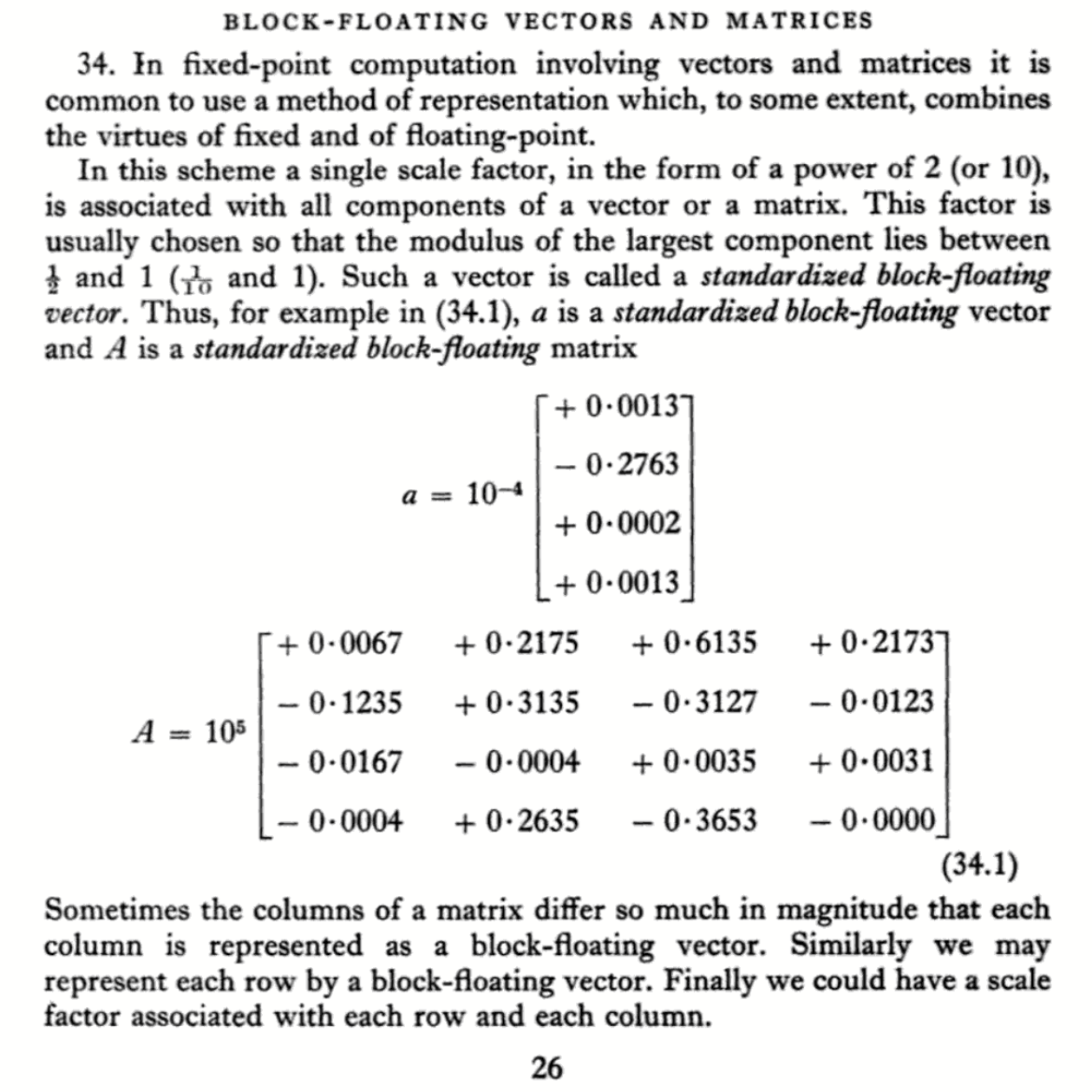
This paper details the Brainwave cloud scale DNN system, top to bottom, including the design of the Brainwave Neural Processor Architecture (NPU) SoC. It reveals the representation trick behind the highly efficient MS-FP datatypes — block floating point formats, recoding vector elements to use a common scaling factor, instead of per-element exponent scaling. This dates back at least to J.H. Wilkinson, “Block-floating vectors and matrices”, pp. 26-27, in Rounding Errors in Algebraic Processes, 1963:
and is implemented, for example, by Chhabra and Iyer in the TI TMS320C54x DSP app note SPRA610, Dec. 1999. Thanks to OGAWA, Tadashi for this reference.
This Brainwave architecture paper is a must-read for understanding hardware efficient (not just FPGA-efficient) approaches to ultra-high throughput, batch size=1, AI tensor math accelerator design. The authors combine many scaling techniques including datapath specialization, hierarchical decode and dispatch, vector parallelism, vector chaining, matrix to vector dataflow, processsing near SRAM, operand reuse, specialized broadcast and reduction networks, and bespoke, narrow precision data types:
“On FPGAs, we employ a narrow precision block floating point format [15] that shares 5-bit exponents across a group of numbers at the native vector level (e.g., a single 5-bit exponent per 128 independent signs and mantissas. … Using variations of BFP, we successfully trim mantissas to as low as 2 to 5 bits with negligible impact on accuracy (within 1-2% of baseline) using just a few epochs of fine-tuning … Using our variant of BFP, no hyperparameter tuning (e.g., altering layer count or dimensions) is required.”
“With shared exponents and narrow mantissas, the cost of floating point (traditionally the Achilles heel of FPGAs) drops considerably, since shared exponents eliminate expensive shifters per MAC, while narrow bitwidth multiplications map extremely efficiently onto lookup tables and DSPs. We employ a variety of strategies to exploit narrow precision to its full potential on FPGAs; for example, by packing 2 or 3 bit multiplications into DSP blocks combined with cell-optimized soft logic multipliers and adders, as many as 96,000 MACs can be deployed on a Stratix 10 280 FPGA.”
#FPGA Update on ms-fp8 etc. Jeremy Fowers’ awesome talk at #ISCA2018 discloses Brainwave uses a block floating point format (e.g. per 128 item vector) in which data are recoded with a single 5b exponent shared by all items + { sign + 2-5b mantissa } per item.
#FPGA This eliminates all those expensive shifters in the dot product adder reduction tree. (Indeed these are the greatest resource use in my reduced precision MAC experiments earlier in this tweet stream.) MS reports as many as 96000 MACs on a Stratix10-280.
#FPGA Block floating point quantization noise is mitigated by a few epochs of DNN model fine-tuning without changing model hyperparameters. This component of the Brainwave work shows for CNN/RNN inference, FPGA LUTs are competitive with hard FPUs in a GPU. Bravo, Microsoft.
Next time, we will revisit this paper below when we turn to the design of RISC-V composable extension(s) for MX data.
Brainwave at NeurIPS 2020
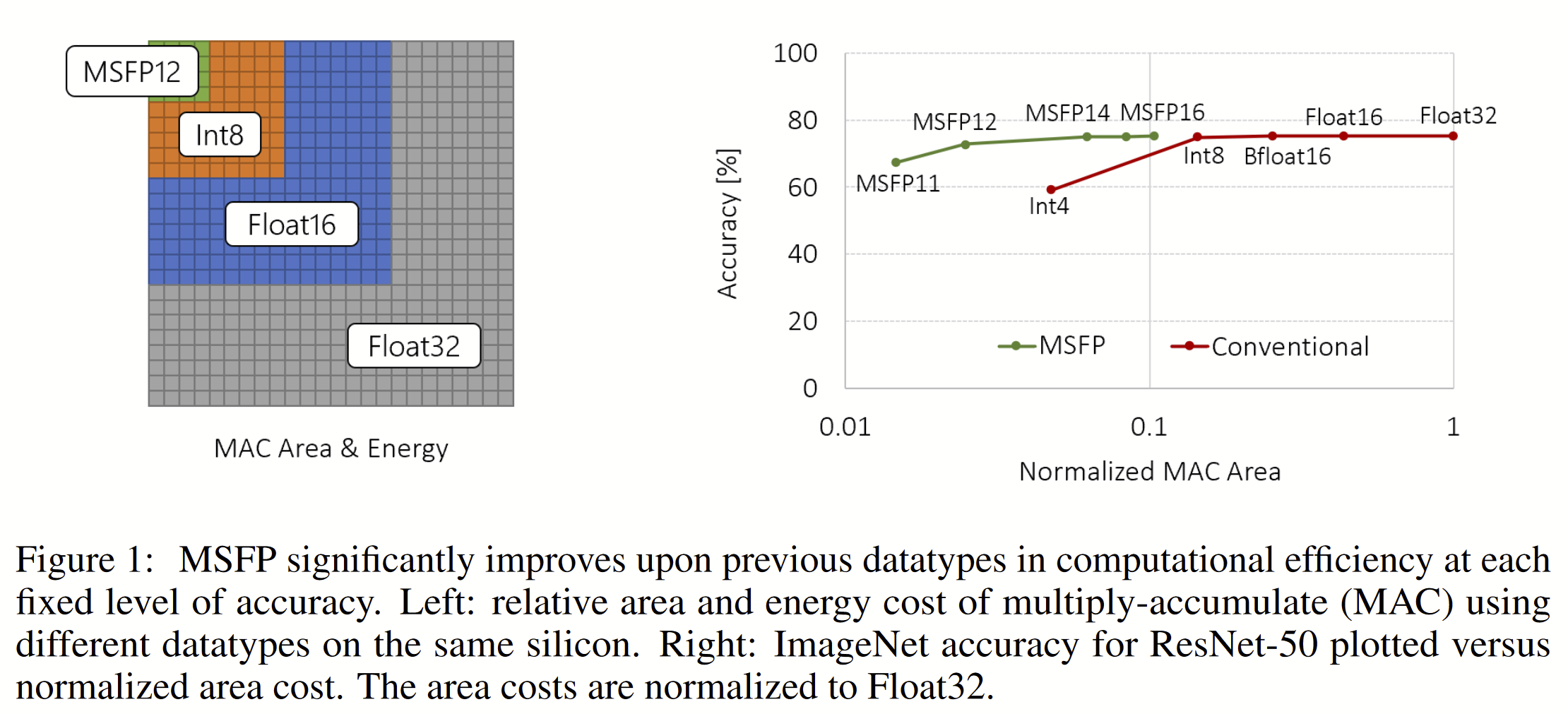
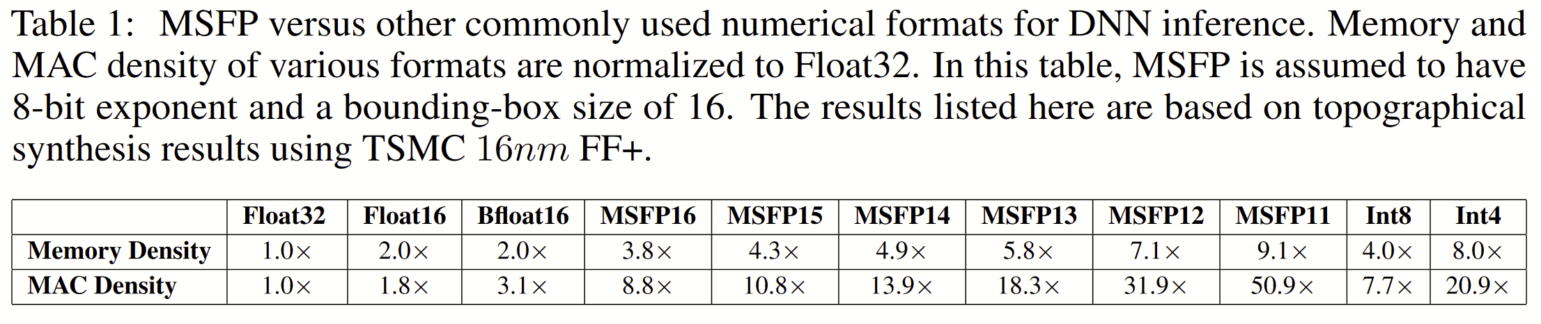
Rouhani et al, Pushing the Limits of Narrow Precision Inferencing at Cloud Scale with Microsoft Floating Point, NeurIPS 2020. DOI. This paper further refines the MS-FP formats from the 2018 paper, and shows “through the co-evolution of hardware design and algorithms, MSFP16 incurs 3× lower cost compared to Bfloat16 and MSFP12 has 4× lower cost compared to INT8 while delivering a comparable or better accuracy.” as illustrated in this figure:
The relative sizes are presented in more detail in this table:
Compelling, right? Compelling enough to justify the extra developer attention, software support, and hardware (quantization and dot products) for these MSFP* formats.
Modern FPGAs with hard block floating point dot product units
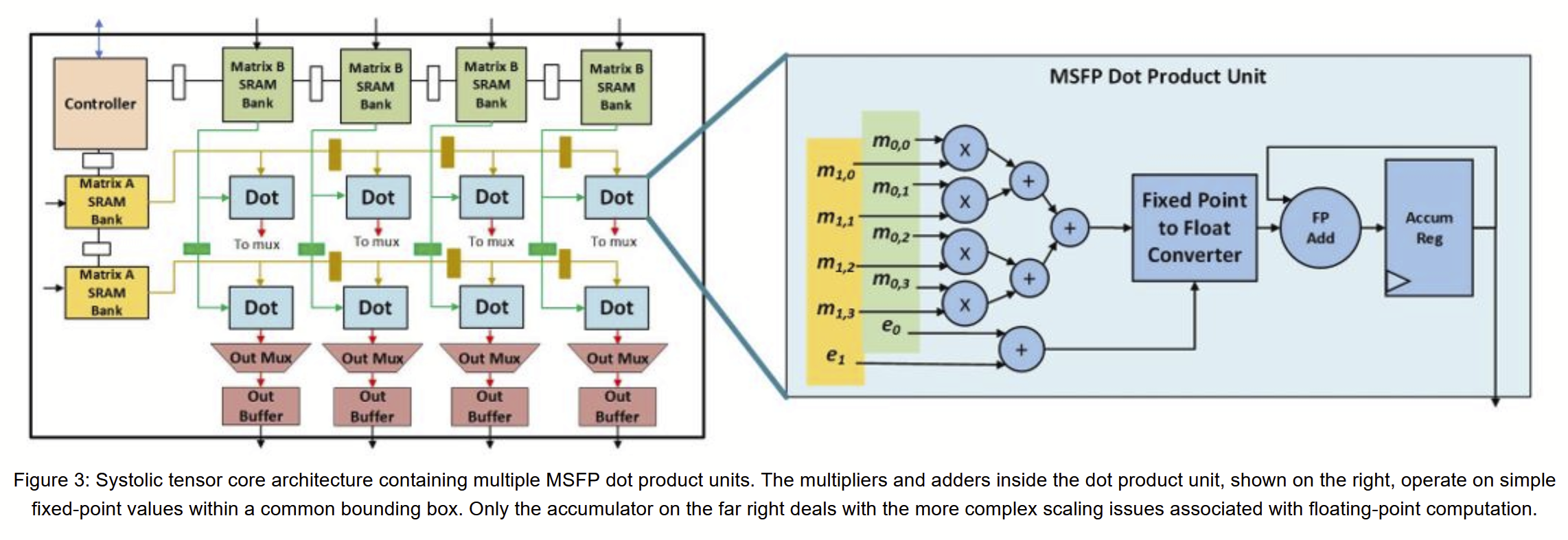
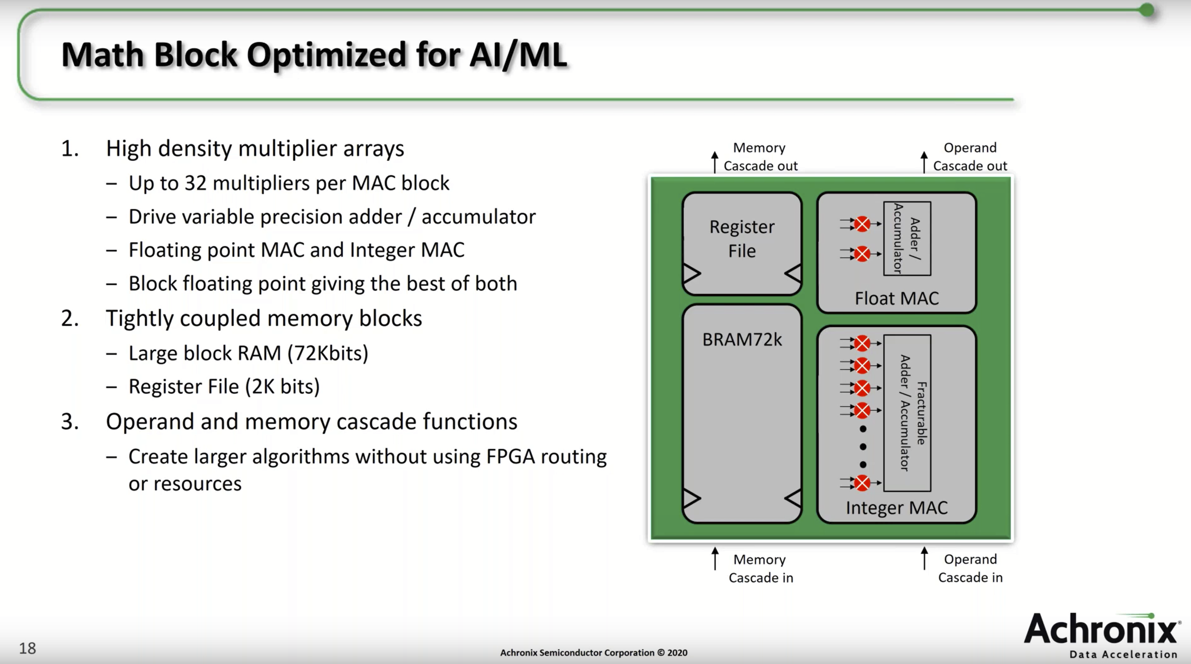
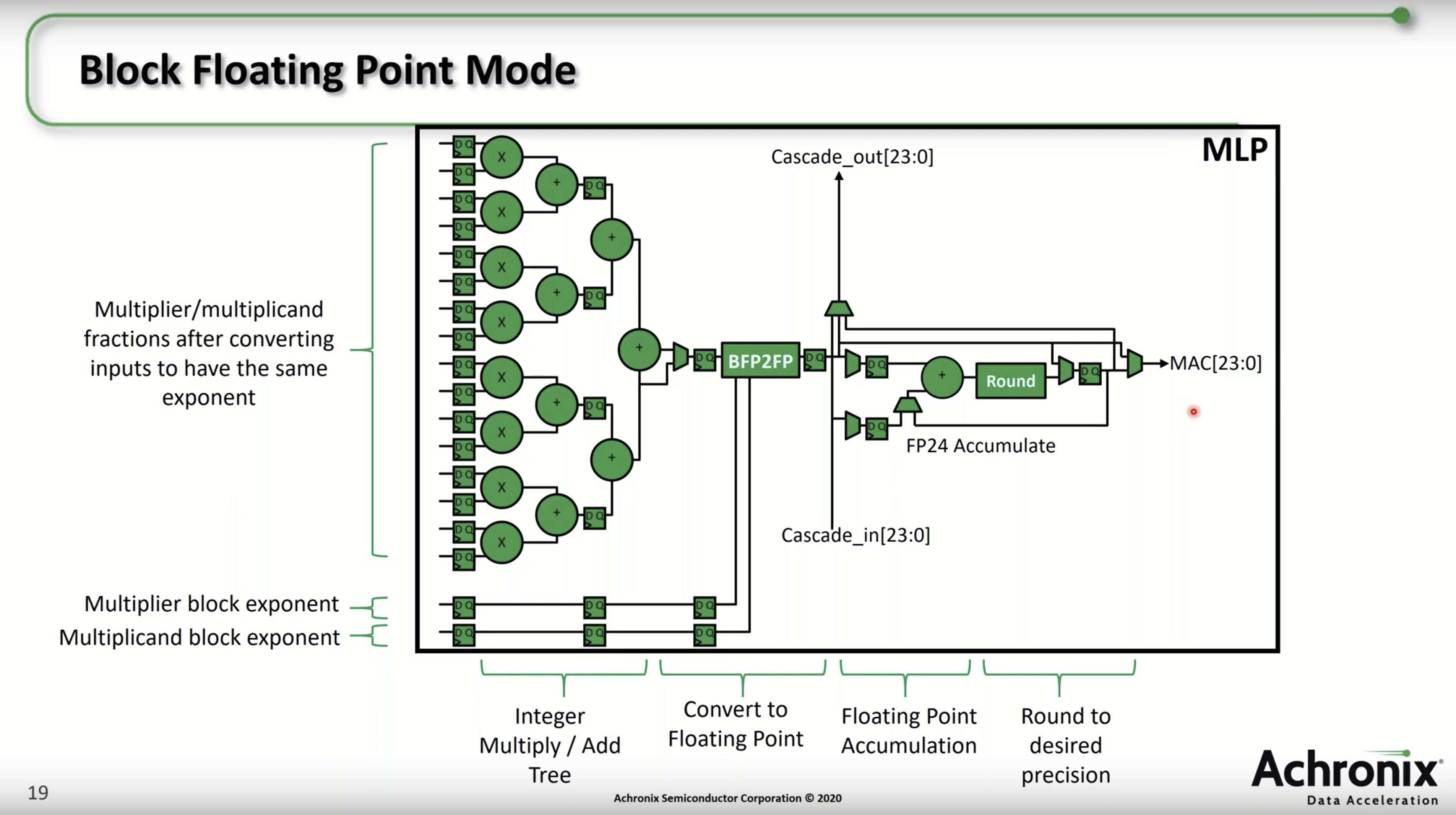
This 2020 Microsoft post also heralds the arrival of hardened BFP dot product units in commercial FPGAs. First introduced in the Achronix Speedster 7t Machine Learning Processor (MLP) blocks in 2019, and then in the Intel Stratix 10 NX (PR)(product brief) in 2020 AI Tensor Block (AITB) units in 2020, these AI tensor math optimized devices provide thousands of hard BFP dot product units. The resemblance to the MSFP Dot Product Unit depicted above is no coincidence. For example, “Working together with our partners in the Intel Programmable Solutions Group (PSG), we’ve delivered significant improvement in area and energy efficiency through silicon hardening”
Below is the Intel AI Tensor Block schematic from the white paper. Each block performs up to 30 8b muls, and 30 adds per clock cycle. A Stratix 10 NX has 3960 AITBs so, if you keep it fed and operating at 600 MHz, it performs 3960 × 30 × 2 ops × 0.6 GHz = 143 TOPS — a double that with a 4b mantissa.
Similarly, new Intel Agilex 5 devices have configurable DSP blocks that implement a streamlined tensor block mode with 10 8b muls + product adds per cycle per DSP. (I would have linked to Intel AITB and Agilex 5 tensor block modes’ detailed specs but it seems Intel does not make that available on the web. Dumb.)
In contrast AMD/Xilinx do not presently implement hard block floating point support in their FPGA fabric, instead providing Versal A.I.Engine (AIE) vector processor arrays.
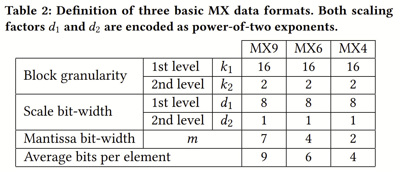
This paper describes a framework Block Data Representations (BDR) to compare the efficiency and quantization loss over a diverse design space of various vector block quantization granularities, with various hierarchies of shared scaling factors, including the 1-level Brainwave block floating point (BFP) formats MSFP*, and novel 2-level shared microexponents (MX) formats, including MX4, MX6, and MX9.
These MX formats are not the MX Alliance formats! Consider Table 2:
If I understand correctly, MX9 is a block of k1=16 elements, all scaled by 2d1, d1 is 8b, further subdivided into 8 subblocks of k2=2 elements, further scaled by 2d2, d2 is 1b, each element being sign × 7b magnitude. In all an MX9 of 16 elements occupies (8b + 8×1b + 16×8b)/16 = 9b per element.
The shared microexponents here contrasts with the present MX Alliance spec, in which each element in an MXINT8, MXFP8 (E5M2 or E4M3), MXFP6 (E3M2 or E2M3), and MXFP4 (E2M1) has a standalone private microexponent (0, 5, 4, 3, 2, 2 bits, respectively).
Or, if you prefer, through the lens of this paper, the MX Alliance MXFP[468] formats are 2-level designs with k1=32 elements, with d1 is 8b, and k2=1 element, with d2 variously 5, 4, 3, 2, 2 bits, respectively.
I wonder what transpired between this ISCA2023 paper and the OCP MX Alliance spec and announcement. I imagine intense multiparty discussions, “can we all please get behind a common MX data schema that evaluates reasonably well on our existing diverse CPUs, GPUs, AIEs, NPUs, etc., that we can evolve future silicon towards, so that we can train our extremely expensive many billion parameter foundational models, just once, and run well on any of them?” If that’s approximately what happened, then any model with k2>1 would probably have been a non-starter. I imagine Microsoft evaluated what became the MX Alliance data formats as part of their BDR parameter sweep and the results were not quite so good as the MX4, MX6, MX9 reported in the ISCA paper, but plenty good enough, in light of this paper, and the MX Alliance white paper: a far superior, drop-in replacement to FP32 and FP16, even for training, and much better QSNR and fewer pitfalls than FP8.
As with the NeurIPS 2020 paper cited above, the evaluations in this paper demonstrate compelling efficiency gains: “MX9 can be used as a drop-in replacement for FP32 or BF16 in the training and inferencing pipeline without the dependency on complex online statistical heuristics or any change in the hyper-parameter settings” and furthermore “MX6 is expected to provide roughly 2× improvement over FP8 in area-memory efficiency and achieves inferences results close to FP32 accuracy with a modest level of quantization-aware fine-tuning.”
The paper also mentions several times the advantages of these MX formats vs. FP8:
“MX9 has a hardware efficiency close to that of FP8 with significantly higher numerical fidelity. For instance, in the case of a Gaussian distribution with variable variance, the QSNR of MX9 is about 16𝑑𝐵 higher than FP8 (E4M3). A 16𝑑𝐵 higher fidelity is roughly equivalent to having 2 more mantissa bits in the scalar floating-point format. For the same distribution, MX6’s QSNR lies between the two FP8 variants E4M3 and E5M2 while providing an approximately 2× advantage on the hardware cost as measured by the normalized area memory efficiency product. We qualitatively observed a similar trend under different data distributions as well.”
Given MX, what FP types are most important in training and inference?
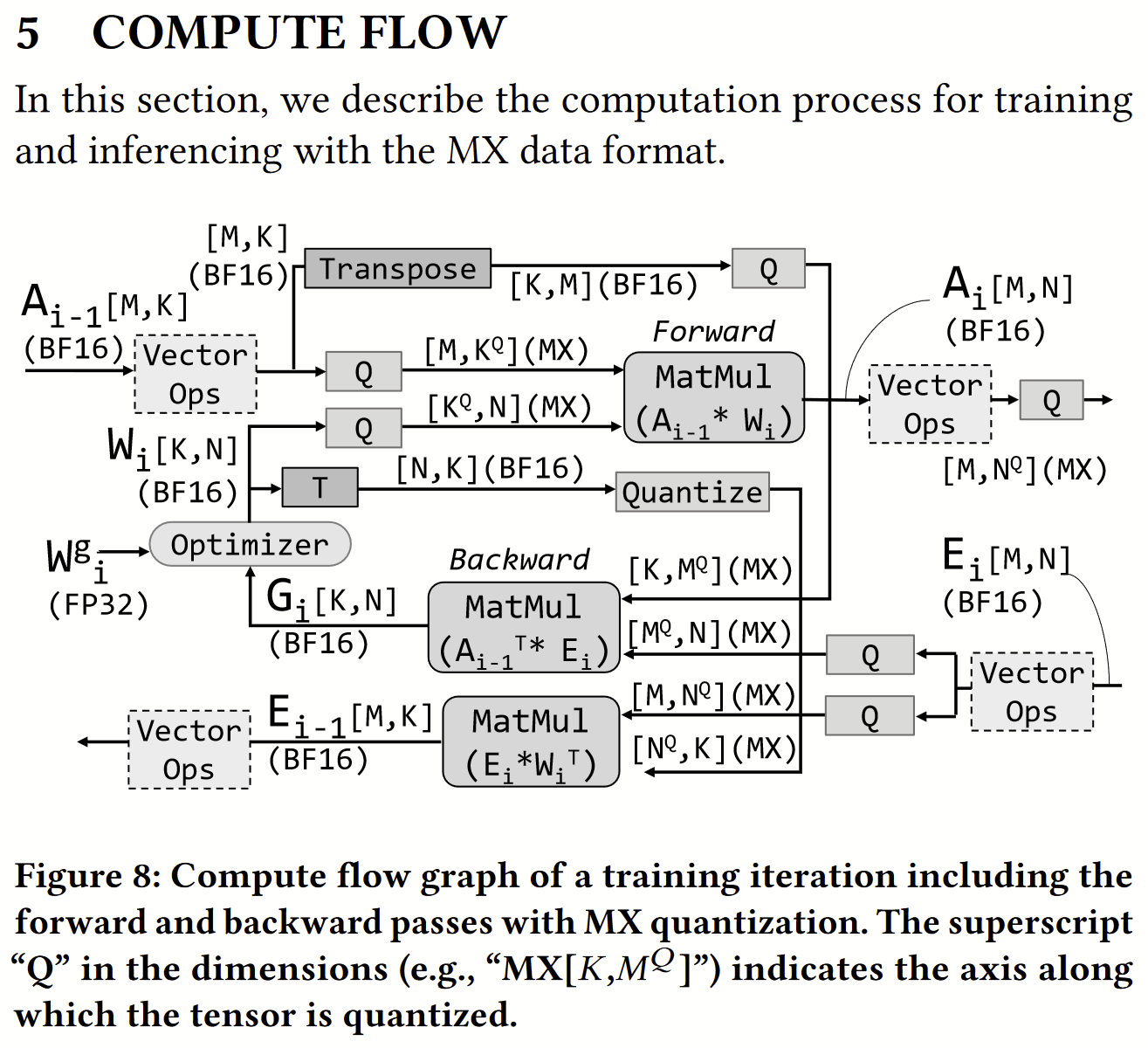
Finally (looking ahead to part two), the paper’s section on Compute Flow is instructive on what kinds of MX data and other reduced precision floating point will be important for ML applications.
Besides myriad MX vector dot products within the MatMuls above, producing BF16 vectors, are quantization operations (along different reduction dimensions) from BF16 to MX, as well as element-wise BF16 vector operations. Is there a need for elementwise MX vector operations, or do MX data live only as fodder for arrays of dot product units within matmuls and convolutions? It seems FP32 and BF16 are necessary: “In our experiments, we use BF16 as the default data format for element-wise operations with the exception of the vector operations in the diffusion loop and the Softmax in the mixture-of-experts gating function.”
It’s also worth noting (section 6.2, Table 4, inferencing) that weights and activations may be kept in different representations (e.g. MX4 weights, MX6 activations) which will merit asymmetric input dot product custom instructions.
Necessity is the mother of invention / “Perspective is worth 90 IQ points”
Wrapping up this part one, some reflection on why it was that Microsoft conceived, refined, perfected, and demonstrated MX format, ahead of all of the other AI focused chip and CSP vendors. Obviously it has much to with Microsoft Research’s decades of work on ML, and then of enterprise and cloud scale ML services, Azure AI services, and Microsoft’s deep expertise operating cloud scale ML workloads, “the world’s computer”, seeing where does the time go and where do the megawatts go.
But for the specific hardware-software codesign insights in MX formats, I think it has a lot to do with their use of FPGAs in Catapult and Brainwave. FPGAs give you a new perspective:
#FPGA Another observation is that although FPGAs are disrespected by elite ASIC designers, the different constraints there afford new insights and spur new approaches that ASIC people may overlook (but ultimately are headed there when the end of Moore’s Law really starts to bite).
#FPGA I used to say you can use today’s FPGAs to build seven year old ASICs — but might also be true that today’s FPGAs help you discover complexity effective design trade offs that will bite ASICs in years to come.
#FPGA Of course things are different in the two worlds — muxes are awful in FPGAs, etc. — but I appreciate the different perspective FPGA implementation affords. “Point of view is worth 80 IQ points” — Alan Kay “I don’t know who discovered water but it wasn’t a fish.”
Gate by gate, wire by wire, FPGAs are often so area and energy inefficient, relative to ASICs, that you just have to find a new, better approach. Those insights can make your FPGA competitive with contemporary ASICs, and give you a leg up when you respin your FPGA design insights into an ASIC of your own. Which Microsoft just did:
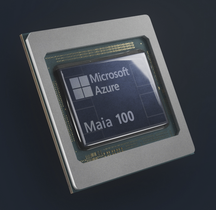
“At Ignite, we’re introducing our first custom AI accelerator series, Azure Maia, designed to run cloud-based training and inferencing for AI workloads such as OpenAI models, Bing, GitHub Copilot, and ChatGPT. Maia 100 is the first generation in the series, with 105 billion transistors, making it one of the largest chips on 5nm process technology. The innovations for Maia 100 span across the silicon, software, network, racks, and cooling capabilities. This equips the Azure AI infrastructure with end-to-end systems optimization tailored to meet the needs of groundbreaking AI such as GPT.”
It’s a lovely thing. Looks like TSMC CoWoS with 4 HBM3 (?) stacks.
“Maia supports our first implementation of the sub 8-bit data types, MX data types, in order to co-design hardware and software,” says Borkar.
In summary
It is a very rare and very special accomplishment for computer architects to define new datatypes that win broad (and TBD: enduring?) industry adoption. Then to go on to design and ship a 100 billion transistor SoC realization of your inventions, a monster with integrated networking and HBM, and advanced packaging, and datacenter scale systems integration! Just stunning. Along the way they also developed Brainwave, the greatest FPGA accelerator that there ever was, and probably that there ever will be. Surely a career highlight for everyone involved. I’m sorry I missed out on all the fun.
Congratulations to Eric Chung, Bita Rouhani, everyone on Catapult, Brainwave, and Maia, and to Microsoft and their partners, on this hardware/software co-design tour de force, the 13+ year harvest of an audacious MSR research agenda and teams built up and tenaciously championed by Doug Burger.
Next time, we’ll explore different approaches to adding MX data type support to RISC-V processors via RISC-V Composable Custom Extensions.
With RISC-V support now from AMD, Intel, Lattice, MicroSemi, and others, FPGA vendors’ transition to RISC-V is (almost) complete. Still a few stragglers.
Related, here for your possible amusement is my IEEE FCCM 2019 Soft Processors Panel presentation, A Game of Soft Processors:
This panel, the same night as the doomed Game of Thrones’ Battle of Winterfell, anticipated a similar wipe out: all FPGA vendors’ proprietary soft processors would eventually fall to the RISC-V juggernaut. This has come to pass. This is good.
The past two decades have been an era of siloed, proprietary, fragmented, duplicative soft processor ecosystems. Use MicroBlaze (or Nios) IP and you were locked in to Xilinx (or Altera) devices.
Now, looking ahead, FPGA vendors should still compete vigorously on best, fastest, smallest processor cores and IP, and most productive development environments, but also, shocker!, they should work together to advance RISC-V standards and profiles for FPGA embedded systems SoCs, so that customer designs are more reusable and portable across platforms. This will be great for customers and great for the vendors, because overall there will be more IP and more solutions ready to run on their latest devices.
RISC-V-standards-based reuse and interop is a major theme and objective of the RISC-V International Soft Processor SIG. Please join us and let’s build a community to advance these standards.
Also, a RISC-V FPGA vendor and user community, together, might speak with a common voice, better to be heard by a RISC-V consortium focused on ASIC design considerations. As RISC-V International undertakes new task groups to shape new standards that address new applications and market segments, the FPGA implementers’ perspective will help ensure that these new standards remain relatively feasible and hopefully economical to implement in FPGAs’ LUTs and BRAMs and DSPs. This is another objective of the SIG:
Background and Motivation
4. FPGA RISC-V systems bring new opportunities and challenges, such as late customizability / fine-grained subsetting, novel memory systems and interconnects, accelerator integration, partial reconfiguration, and alternative arithmetic systems, that may not be a priority or relevant to ASIC implementations.
5. Proposed RISC-V ISA extensions may inadvertently induce circuit structures that are prohibitively expensive in certain FPGA devices or use cases. …
Goals and Scope
2. Represent FPGA implementation considerations within RISC-V TGs, acting as a resource for consultations and to monitor progress of RISC-V standards from the perspective of Soft CPUs.
We presented a poster(narration) on this work at the 2022 Paris RISC-V Summit. Then we stepped back, to work elsewhere, and waited to see if there were new interest or uptake in the work. Some but no groundswell!
I did some development work towards that first still-pending end-to-end composition demo. I added some example CFUs to the nascent CFU Zoo, including implementations of the three CFU-LI level adapters and a CFU Switch.
SIG-SOFT-CPU was one the original RISC-V Foundation SIGs. In 2019 our focus (and teleconf meetings) gradually devolved to strictly focus on refining the composable custom extensions work and so the other SIG charter items received short shrift. With the transition to RISC-V International, SIG-SOFT-CPU went dormant, but now in summer 2023, Guy is working to reboot the SIG. Currently he is driving a process to ratify a new Charter for the SIG.
The great big rename: goodbye Custom Interfaces and Custom Function Units (CFUs), hello Composable Extensions and Composable Extension Units (CXUs)!
For better or worse, the Custom Extensions spec has always used the invented, defined term Custom Interface to mean the abstract immutable interface contract of a composable custom extension. From the beginning I used this term because 1) it shone a spotlight on the all-important interface contract aspects of a custom extension, and 2) as homage to its inspiration, Microsoft COM Interfaces. Unfortunately it has only sowed confusion, between terms Custom Interface and Composable Extension, particularly because the spec also uses the (separate) concept interoperation interface extensively.
At last week’s online meeting I gave a 45 minute deeper dive into Composable Extensions for the SIG-SOFT-CPU members. When prepping for this talk, and giving it, I was frustrated that these particular monikers were not helping to convey concepts and understanding. It was time to say goodbye to custom interface. We needed a new term (not custom extension) to distinguish the category of composable custom extensions from current non-composable custom extensions and I chose composable extension for short.
This anticipates a RISC-V ISA world with standard extensions, composable extensions, and custom extensions; CX ::= composable extension.
Similarly we need a crisp term for the reusable modular hardware unit that implements a composable extension. Years ago I coined the term custom function unit for this type of tightly CPU-coupled synchronous hardware unit, because it implements the custom function instructions of composable custom extensions. But CFU is no longer apt and ideal. For one thing, an early fork of our group’s CFU and CFU logic interface design have become extensively used in the CFU Playground work. It seems tiring, hopeless, and pointless to try to wrest back the CFU moniker imprimateur from the CFU Playground folks for the present composition focused work.
Thus throughout the spec custom function unit (CFU) becomes composable extension unit (CXU). This is appealing because it captures its relationship to CXs: a composable extension unit is a core that implements a composable extension. Perfect. Also, and I can’t explain why, for me, CXU suggests a core that is different more flexible and powerful than a mere CFU. (Beyond older CFUs, proposed CXUs enable uniform/automatic: composition, n state contexts, OS context switching, multicore CPU complexes, extension versioning, …)
I hope you enjoy it, and find it a helpful complement to the spec.
The last slide, our Call to Action, proposes the next step in the work, which is, working with the RISC-V International framework, that the SIG-SOFT-CPU SIG should sponsor two new RVI Task Groups, an ISA TG to standardize -Zicx (custom extension multiplexing) and a non-ISA TG to standardize CXU-LI (custom extension unit logic interface).
A 2000 LUT configuration, implemented with Openlane
Here is the first implementation of the S3GA<N=2048,M=8,K=4> design, which fits in the efabless Open Shuttle Program‘s ~10mm2caravel_user_project area (2.92mm x 3.52mm) for the 130nm Skywater PDK, as produced by the wonderful OpenLane tools.
GDS-II plot of the first version of the S3GA<2048> design, implemented in 130nm sky130 process.
Implementation plus signoff checks take about 7 hours. At peak the tools used 60 GB of RAM. There are 2 wee Magic design rule check failures to investigate. Some design stats: 141,000 DFFs, 14,000 mux4s and 19,000 mux2s. This first cut has a 9 ns clock period = M=8-cycles at 72 ns = 14 MHz.
Next: DFFRAM?
This design uses 256-4=252 eight 4-LUT logic blocks (LB8s) (see part one), each of which uses an 8x48b configuration memory — an 8-entry x 48b circular shift register.
I hope to replace the hundreds of 8x configuration memories with bespoke, placed (floorplanned) instances of DFFRAM macros. This should also make it more practical to add a LUT-RAM mode to LB8s, so they may also be used as true dual port 32×8 SRAMs and possibly as 2R1W-64×4 SRAMs. Thus each X32 tile could implement a 32×32 register file.
It should also be possible to replace some X128 tiles with 100% DFFRAM or OpenRAM based block RAM (BRAM) cells at >3x the density of S3GA LUT-RAM.
Note: this blog post is under construction. This notice will be removed when it is complete.
Introduction: a look back at S4GA
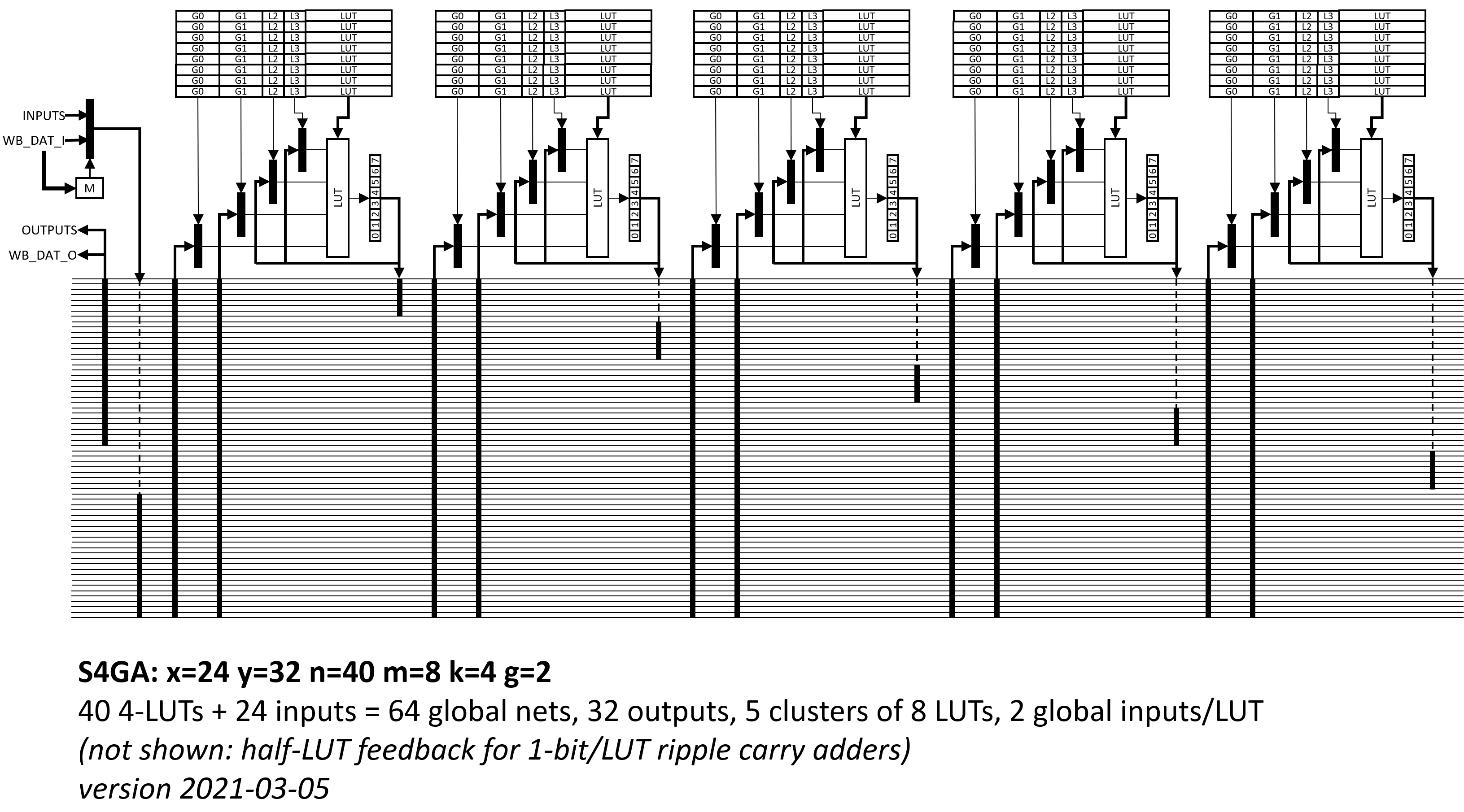
In winter 2021 I took the first edition of Matthew Venn’s superb Zero to ASIC course. My 300x300um project was S4GA: “a small simple slow serial” FPGA core, targeting ~0.1mm2 of the 130nm Skywater ASIC PDK, using the efabless Caravel harness and the Zero-to-ASIC multiproject framework. This core fit an N=40 4-LUT (four input lookup table) FPGA arranged in 5 clusters of M=8 LUTs, with a full cluster cycle time of M=8 cycles. A family tragedy interrupted this work and I did not finish it nor submit to MPW-1.
Block diagram of the N=40 M=8 K=4-LUT S4GA FPGA designed for the Zero-to-ASIC course (2021)
GDS plot (300um x 300um) of the Skywater130 implementation of the S4GA core, N=40 M=8 K=4-LUTs
Scaling way up with S3GA
Now I am reworking S4GA into a much larger (N>1000 LUTs) FPGA for the upcoming efablessMPW-8 run, closing Dec. 31, 2022. A full efabless Caravel user project area is over 10mm2, approximately 100x larger than this earlier N=40 design.
As this new FPGA core won’t be small, nor (in the spatial computation sense) slow, it is reborn as S3GA — simple scalable serial FPGA. (Pronounced “see-gah”, not “say-gah”.)
“What do you mean by serial FPGA?” The FPGA evaluates N logical LUTs using only N/M real LUTs, over M cycles. A serial FPGA trades off latency (e.g., logical clock period) for greater capacity by sharing (amortizing) the gate and wiring area of lookup table input and output multiplexers (muxes).
For S3GA, one LUT Block of M=8 logical K=4-LUTs (“LB8”) contains eight 4-LUT contexts (each about 40b, see below), and one physical 4-LUT (including one or more logic block input muxes, four LUT input muxes, one 16:1 LUT output mux, and a flip-flop output mux).
The README of the old N=40 S4GA design is instructive. Take a look. For that design:
N=40 and M=8, so across the whole design, this S4GA configuration evaluates 5 LUTs per cycle, or 40 LUTs per 8 cycles.
The global interconnect is just a flat 64b bus that passes each cluster. Each cluster has G=2 64:1 muxes to select two global input nets per LUT per clock.
Contemplating S3GA, with perhaps 50x more more LB8s and LUT outputs, this flat global interconnect architecture will not scale. For example, it could mean running 1000-bit buses past hundreds of LB8s and many hundreds of 1000:1 input muxes, and so forth. Such a flat design would also be over-provisioned with so many mm2 of unneeded global wiring and super wide LUT input muxes.
Rent’s Rule, T=tgp, estimates T (number of external IOs) as a function of g (number of gates), t and p constants, p<1, sometimes p=~0.5. It reflects that most of a circuit’s sub-circuits’ nets remain local to that sub-circuit — recursively so in a hierarchical design. For an FPGA architecture that hosts real world N LUT digital circuits, tNp global nets, instead of N global nets, will usually suffice. Also, within any subset of M k-LUTs of a circuit, there are never more than Mk inputs and M outputs.
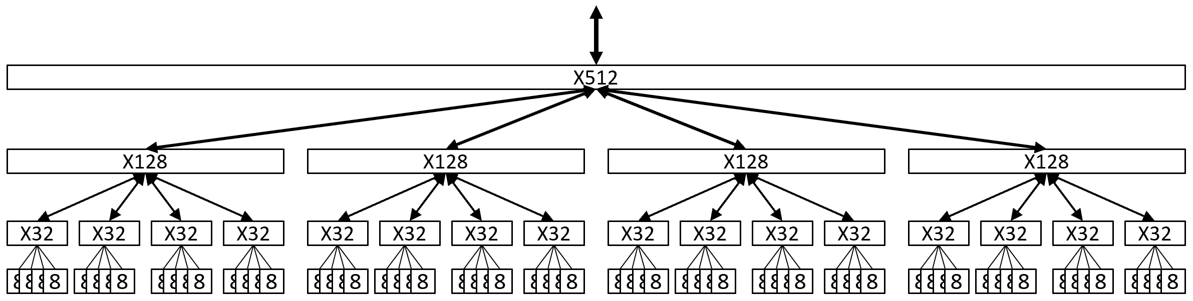
Connecting a hierarchy of clusters
Instead of a classic island-style FPGA of rows and columns of M k-LUT clusters and switchboxes, S3GA will be a hierarchy of LB8s, clusters of LB8s, etc., interconnected with a hierarchy of switches in a fat tree like interconnect. This should allow a relatively simple place-and-route CAD flow to transform synthesized, technology mapped K-LUT netlists into S3GA configuration bitstreams.
Anticipating a 2D physical design layout, we arbitrarily pick a sub-cluster branch factor of four, so that sub-clusters may be (recursively) floorplanned to NW, NE, SW, SE quadrants of each cluster.
Here’s a sketch of a N=512 logical LUT quadrant of such a design:
A hierarchical N=512 LUT quadrant of a large S3GA FPGA
At the leaves of this quadrant are sixty-four LB8s, each labeled 8. LB8s (hence LUTs) only appear at the leaves of the graph.
Each cluster of four LB8s is composed by an X32 switch. The X32 switch routes some subset of its 32 LUTs’ outputs up to its parent X128 switch, accepts some inputs from its X128 switch, and routes them down to its four LB8s as appropriate.
At the next level up, the X128 switch accepts subsets of LUT outputs from its four child X32 switches, as well as other input nets from its parent X512 switch, and routes input subsets of all these nets down to its four child X32 switches.
At the top level of this diagram, the X512 switch accepts subsets of LUT outputs from its four child X128 switches, as well as other inputs nets from its parent X2048 switch (not shown), and routes input subsets of all these nets down to its four child X128 switches.
With this architecture, global LUT placement is (mostly) finding the minimum cut 4-partition of the netlist hypergraph, and repeating min cut 4-partitions recursively until each subpartition fits in an LB8. A design “fits” into the device if its LUTs fit into the total LB8 capacity of the device, of course, and if the size of each cut is not greater than the capacity of the corresponding inter-switch bus. Following a successful hierarchical partitioning, routing requires scheduling which LUTs to evaluate in which cycles, and filling in so many input and output mux selection tables.
Reflecting Rent’s rule, the switch hierarchy need not “route up” every LUT output. For example, an LB8 might have 8 outputs to its parent switch, and the X32 switch might have 32 outputs, but the X128 switch might output only 64 of those 128, and the X512 switch might output only 128 of those 512.
Similarly, for input routing, an X128 switch might “route down” (different) 48 net subsets of its input nets for each of its four child X32 switches. (Specific switch I/O bus width parameters are TBD.)
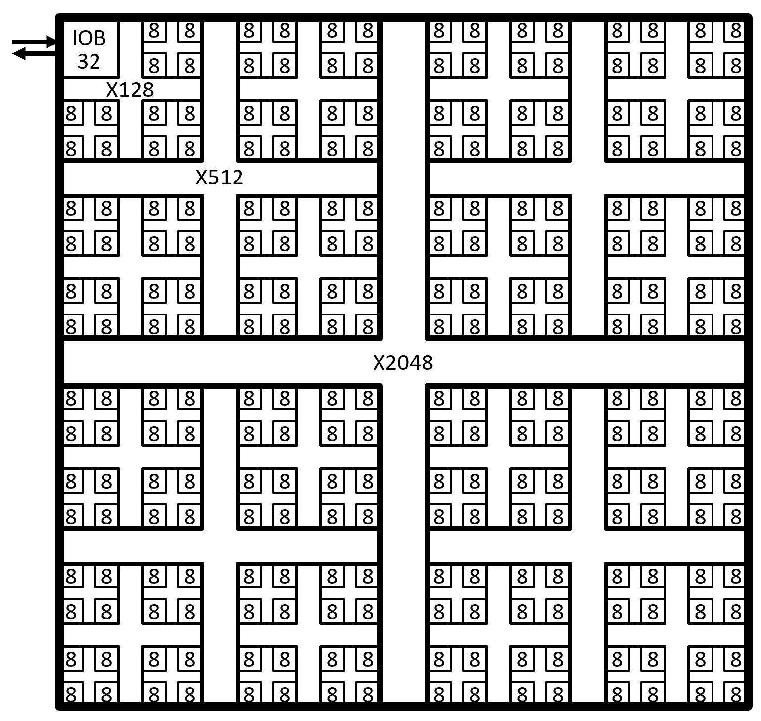
Floorplan
Here is an example floorplan for a N=2048 LUT S3GA device, reflecting the proposed recursive 2D 4-partitioning of the circuit. The first leaf cluster of four LB8s (32 LUTs) is replaced with a 32b IO block (“IOB32”).
Floorplan of a 2K LUT S3GA
Observe that a LUT output net from one LB8 to an adjacent LB8 at the same X32 switch need never leave that domain, whereas a LUT output in some X512 quadrant may be received as a LUT input in some other other X512 quadrant, by ascending an X32, X128, and X512 switch, up to the top-level X2048 switch, then descending an X512, X128, and X32 switch, down to the receiving LB8.
A serial interconnect fabric
S3GA’s LB8’s bit serial nature economizes standard cells per logical LUT. More significantly, it enables a remarkably frugal programmable interconnect fabric.
Referring to the older N=40 S4GA block diagram figure above, the five M=8 LUT clusters are passed by a bus of 64 nets (24 FPGA inputs and 40 LUT outputs). But each of these 40 LUT output wires changes only once per M=8 cycles. These 40 LUT outputs could be conveyed over five wires by serially streaming out LUT outputs into the interconnect fabric. Now the LUT input muxes that select input values from these LUT outputs can be just a (5-1):1 mux instead of a (40-8):1 mux. Now transmitting all 128 LUT outputs from a X128 switch quadrant requires only 16 wires (over 8 clock cycles). Now selecting one of these 128 outputs requires a 16:1 mux instead of a 128:1 mux (i.e., five mux4_1s cells instead of 42+ cells).
However serial transmission of LUT outputs on shared wires significantly complicates LUT cycle scheduling. If LUT A in some LB8 has an output net that is an input of LUT B in an adjacent LB8, it is necessary to schedule the LUT B evaluation one cycle after the LUT A, because that is the only clock cycle during which the A value is available on a LUT output wire. Use it or lose it! But if LUT B has a second input, LUT C, evaluated during a different clock cycle than LUT A, there is no clock cycle during which A’s and LUT C’s outputs are simultaneously available as LUT B inputs. Drat. We’ll address this problem momentarily.
So across the entire hierarchical interconnect fabric, S3GA conveys all LUT output nets in the M=8 serial time domain, eliminating (M-1)/M of all wires and their mux trees.
The serial interconnect fabric hierarchy
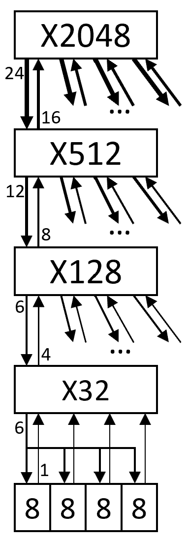
This figure revisits the N=512 LUT quadrant hierarchy figure above, labeling the switch input and output ports with strawman port widths, for one vertical slice of elements through the hierarchy. Remember these port widths are for bit serial ports, and convey, across eight clock cycles, eight times as many nets as port wires. For example, the four 16-wire ports that are the inputs of the top level X2048 switch, carry 4x16x8 = 512 output nets from the four X512 quadrants.
A slice through the switch hierarchy, labeled with serial interconnect I/O bus widths.
This table summarizes the strawman switch port width parameters.
Parameter
Value
Description
N
2048
no. of LUTs (incl. IOB32 as LUTs)
M
8
no. of logical LUTs per LUT (or, per logic block)
B
4
branching factor: no. of sub-clusters per cluster
O0
1
level 0: LB8: no. of serial outputs
O1
4
level 1: X32: no. of serial outputs
O2
8
level 2: X128: no. of serial outputs
O3
16
level 3: X512: no. of serial outputs
N4
64
level 4: X2048: no. of serial nets
I3
24
level 3: X512: no. of serial inputs
I2
12
level 2: X128: no. of serial inputs
I1
6
level 1: X32: no. of serial inputs
I0
9
level 0: LB8: no. of serial inputs
LB8 input deserialization
When a serial LUT output net is routed to and arrives at some LB8, it is selected as an LB8 input by one of I >=1 logic block input muxes, whether or not the net is an input for the logical LUT evaluation that cycle. This input net is buffered in one of I (M-deep) LB8 input buffers (serial-in parallel-out shift registers). This input net value may then be used as a LUT input during the next M LUT eval cycles of that LB8.
In the baseline (bit parallel interconnect) S4GA N=40 M=8 LUTs design, there are G=2 global inputs per LUT cluster, using two 40:1 muxes (each 13 mux4_1s). Adopting a bit serial interconnect and LB8 input deserialization, there are two 8:1 LB8 input muxes, two 8x1b LB8 input buffers, and two (8+8+…):1 LUT input muxes (5+… mux4_1s), each selecting a LUT input from the LB8 input buffers.
The base S4GA design requires M=8 x G=2 x clg(40) bits = 96b of configuration data to select two LUT inputs from the 40 bit parallel LUT outputs, whereas the bit serial version requires M=8 x I=2 x clg(5) bits = 48b of configuration data (LB8 inputs) plus M=8 x I=2 x clg(8+8+…) = 80b of config data for two LUT input selectors (LUT inputs). A 60% increase — worth it to mitigate LUT cycle scheduling constraints.
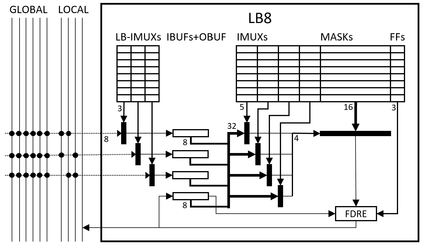
Level 0: M=8 logic block (LB8)
This figure shows the general structure of the M=8 I=3 K=4 logic block (“LB8”), now with block input muxes and buffers.
Architecture of LB8: M=8 I=3 K=4 LUT block
(Not shown: configuration logic, half-LUT cascade, D-FF clock enables and set/reset, and 32×8/64×4/128×2/256×1 true dual port RAM mode.)
At left, the block is passed by six global wires and four local wires. Global wires are serial input nets from afar, received via the block’s X32 switch. Local wires are the serial output nets of the four LB8s in this X32 cluster.
Each cycle the block inputs three of these nets, as selected by three 3b LB-IMUX selector fields. These three inputs are buffered in three 8b IBUF shift registers. Together these 24b plus the most recent 8 LUT outputs (the OBUF shift register) are the 32 possible input nets for the 4-LUT.
Next, four 5b IMUX selector fields select four of these 32 inputs as the 4-bit LUT input. This selects one of the 16 bits of the LUT mask as the LUT combinational output.
Then, the final output of the LUT net is determined by combinational output, the previous value of the LUT output (i.e., the M=8 shift-out bit of OBUF), the global reset input (not shown), the LB8 clock enable (CE) input (not shown), and the LUT’s 3b FF control field.
The new value of the LUT output net is captured in the OBUF shift register, and is output via a local wire to the other LB8s in this cluster, and to the X32 switch.
In an N=2048 LUT S3GA, 256 LB8s – 4 LB8s (IOB32) require about 252 x (8×48 + 32 + 4) = 252 x 420 = 105,840 configuration bits.
LB8 half-LUT cascade
Half-LUT cascade is a simple local optimization to implement adders efficiently. A n-bit ripple carry adder comprises a vector of n full adder cells. Each cell adds a[i], b[i], and carry[i-1], producing sum[i] and carry[i]. When this is technology mapped to a pure 4-LUT FPGA, it requires 2n LUTs for the 2n LUT outputs (sum[n-1:0] and carry[n-1:0]).
S3GA LB8’s provide half-LUT cascade to implement n-bit adders in n LUTs. S3GA provides a simple fracturable LUT, treating a k-LUT as two (k-1)-half-LUTs of the same k-1 inputs. So in addition to the usual full k-LUT output, which can be routed anywhere in the S3GA, an additional half-LUT (i.e., (k-1)-LUT) output, using the k-1 LSBs of the LUT input index, is also evaluated and registered in a “half_q” register for possible use as the half-LUT cascade-in in the next tick.
For example, when k=4, LUT inputs { 1’b1, half_q, b[i], a[i] } can index an adder LUT mask that produces sum[i] as the output of the full LUT (i.e., the upper half LUT) and carry[i] as the output of the lower half LUT. To select a half-LUT cascade input and half-LUT evaluation, a LUT’s k-1 and k-2 LUT input selectors are set to all-ones. The first special selector selects a constant 1; the second selects the current value of half_q.
To facilitate wide adders (up to n=32b in 32 LUTs / 4 LB8s), starting in any LB8, the half-LUT output of LUT #7 in each LB8 cascades into the half-LUT input of LUT #0 in the next LB8 in the four LB8-cluster. For those of you (properly) thinking serially, that means, in tick M-1=7, that the half-LUT output of each LB8 is registered as the next half-LUT input, for (pending) tick 0, in each next LB8 in the cycle (LB8 #0, #1, #2, #3, #0, …). Of course, unless adder sub-segments are pipelined, a ripple-carry 32b add still has a latency and an initiation interval of 32 ticks = 4 tocks.
TODO: illustrate half-LUT carry adders with a figure and LUT netlist.
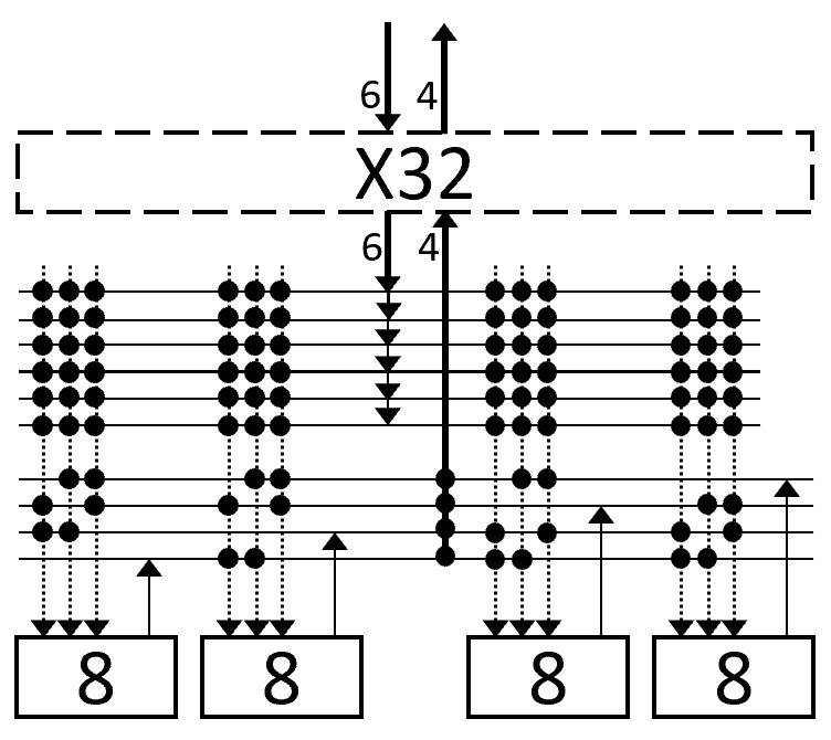
Level 1: Composing four LB8s with a (transparent) X32 switch
Four LB8s composed by a (transparent) X32 switch
In an N=2048 LUT S3GA, 64 X32s require zero configuration bits and zero muxes.
Level 1: IO block (IOB32)
The first (and only, for the time being) “X32 switch cluster” of four LB8s is replaced with an IOB32 block. This interfaces the serial interconnect S3GA with the greater parallel interconnect SoC. It consists of a configurable input crossbar selecting up to 32 inputs into a 4b serial output bus, plus a configurable output crossbar, receiving a 6b serial input bus and from that selecting and registering up to 48 parallel outputs.
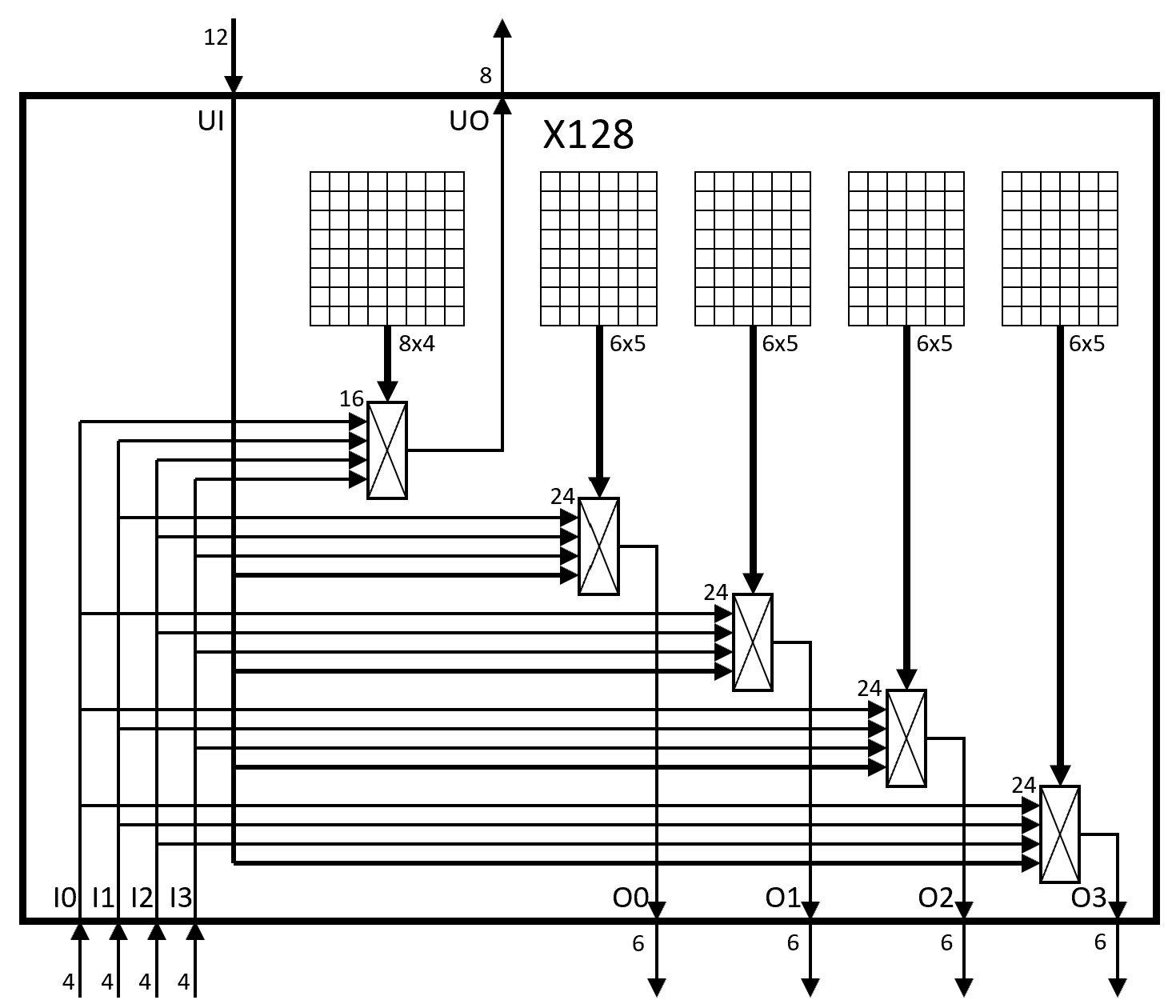
Level 2: Composing four X32s with an X128 switch
Architecture of an X128 switch
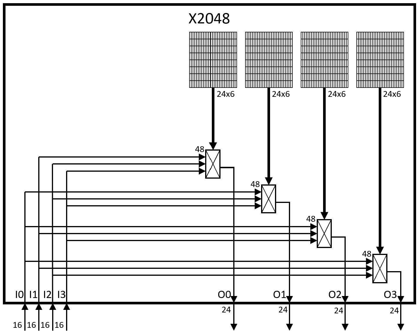
In an N=2048 LUT S3GA, sixteen X128s require 16 x (8x8x4 + 4x8x6x5) = 16 x 1,216 = 19,456 configuration bits and 16 x (8×16:1 + 4x6x24:1) muxes = 16 x (8×5 + 24×8) mux4_1s = 16 x 232 mux4_1s = 3,712 mux4_1s.
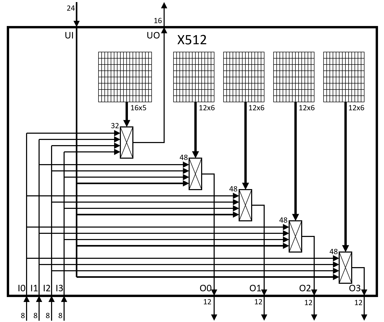
Level 3: Composing four X128s with a X512 switch
Architecture of an X512 switch
In an N=2048 LUT S3GA, four X512s require 4x (8x16x5 + 4x8x12x6) = 4 x 2,944 = 11,776 configuration bits and 4 x (16×32:1 + 4x12x48:1) muxes = 4 x (16×11 + 48×16) mux4_1s = 4 x 944 mux4_1s = 3,776 mux4_1s.
Level 4: Composing four X512s with a X2048 switch
Architecture of an X2048 switch
In an N=2048 LUT S3GA, one X2048 requires 4x8x24x6 = 4,608 configuration bits and 4x24x48:1muxes = 96×16 mux4_1s = 1,536 mux4_1s.
Today’s The Register article by Agam Shaw, RISC-V takes steps to minimize fragmentation, discusses RISC-V International’s efforts to grapple with the RISC-V instruction set architecture’s growing pains as its diverse community strives to apply and optimize RISC-V to many different use cases.
There is a fundamental tension between development of new RISC-V optional standard extensions which must be non-proprietary, of broad interest and general utility, which may take years to reach consensus and ratification, and which consume a shared, limited resource (RISC-V encoding space and overall complexity), versus development of a custom extension, which may be the work of one party, in house, in one day, narrowly targeted, and/or proprietary. Both are valuable and necessary. However, RISC-V does not currently provide means to make these custom extensions, their hardware implementations, and their software libraries, reusable and interoperable, which does silo solutions and fragments the ecosystem.
Imagine you could combine the guaranteed correct composition of the optional standard instruction set extensions, and the agility of custom extensions. For several years, a small group of RISC-V FPGA soft processor developers and users have met informally, on and off, working towards this vision.
This first edition of the spec focuses on the prerequisite common HW-HW and HW-SW interfaces, formats, and metadata required to achieve robust automatic composition of custom extensions. Notably the spec includes a chapter on the Custom Function Unit Logic Interface, a HW-HW interface for composable custom function units that plug-and-play into different processors and systems. Beyond this spec, much work remains to define the software stack and software tooling above these interfaces, flesh out the Runtime, etc.
We just submitted a one page abstract for a poster which we hope may be presented and discussed at the upcoming 2022 Spring RISC-V Week in Paris. If the 50 page spec is daunting, this one page TLDR abstract attempts to provide a brief overview of some objectives and contributions of the work.
To get involved with this work, stay tuned, we will set up a public mailing list for discussions momentarily (and update this paragraph). Also please raise your spec concerns and suggestions in the Issues list. Thank you for your interest. Onwards!
Whenever we specify new a custom extension, implement it as a custom function unit, or target it as an accelerated library, let us do so using common, standardized interoperation interfaces so that it may “just work” with all RISC-V CPUs and the other standard and custom extensions.
Composable Custom Extensions and Custom Function Units for RISC-V (Poster Abstract submited for 2022 Spring RISC-V Week)
Jan Gray (Gray Research) , Tim Vogt (Lattice Semiconductor), Tim Callahan (Google), Charles Papon (SpinalHDL), Guy Lemieux (University of British Columbia), Maciej Kurc (Antmicro), Karol Gugala (Antmicro)
This poster introduces a draft specification for composable custom instruction extensions in RISC-V. The RISC-V custom instruction encoding space is unmanaged, leading to potential conflicts when combining different accelerators and their libraries into one system. This specification defines interop interfaces including a physical logic interface and CSRs that manage the composition of multiple, independently developed custom instruction extensions. Contributions include custom interface multiplexing and stateful but isolated state for multiple harts sharing multiple custom function units (CFUs).
Today, custom extensions don’t interoperate
SoCs may use app-specific hardware accelerators to improve performance and energy – particularly so with FPGA SoCs that offer plasticity and abundant spatial parallelism. The RISC-V ISA explicitly supports domain-specific custom extensions.
There are many RISC-V processors with custom instruction extensions, and now some vendor tooling. But the accelerated libraries that use these extensions and the cores that implement them are authored by different organizations, using different tools, and may not work together. Different custom extensions may conflict in use of opcodes, or their implementations may require different CPU cores, pipeline structures, logic interfaces, models of computation, means of discovery, context switching, or error reporting. Composition is difficult, impairing reuse of hardware and software, and fragmenting the RISC-V ecosystem.
Unleashing innovation in interoperable custom extensions
RISC-V International uses a community process to define a new standard extension to the RISC-V ISA. New extensions must be of broad interest and utility to merit allocation of precious RISC-V opcode space, CSR space, and generally to add to the enduring complexity of the platform. New extensions typically require years to reach consensus and ratification. Each coexists with all other extensions. Might any new custom extension also safely coexist (compose) with all extensions? Might there be a rich ecosystem of plug-and-play custom extensions? Yes!
Our proposed interop interfaces allow any party to rapidly define, develop, and use:
a custom interface (CI): a custom extension consisting of a set of custom function (CF) instructions,
a custom function unit (CFU): a composable hardware core that implements a custom interface,
an accelerated CI library that issues custom instructions,
a processor that can mix and match any CFUs (plural), and
tools to create and compose these elements into systems.
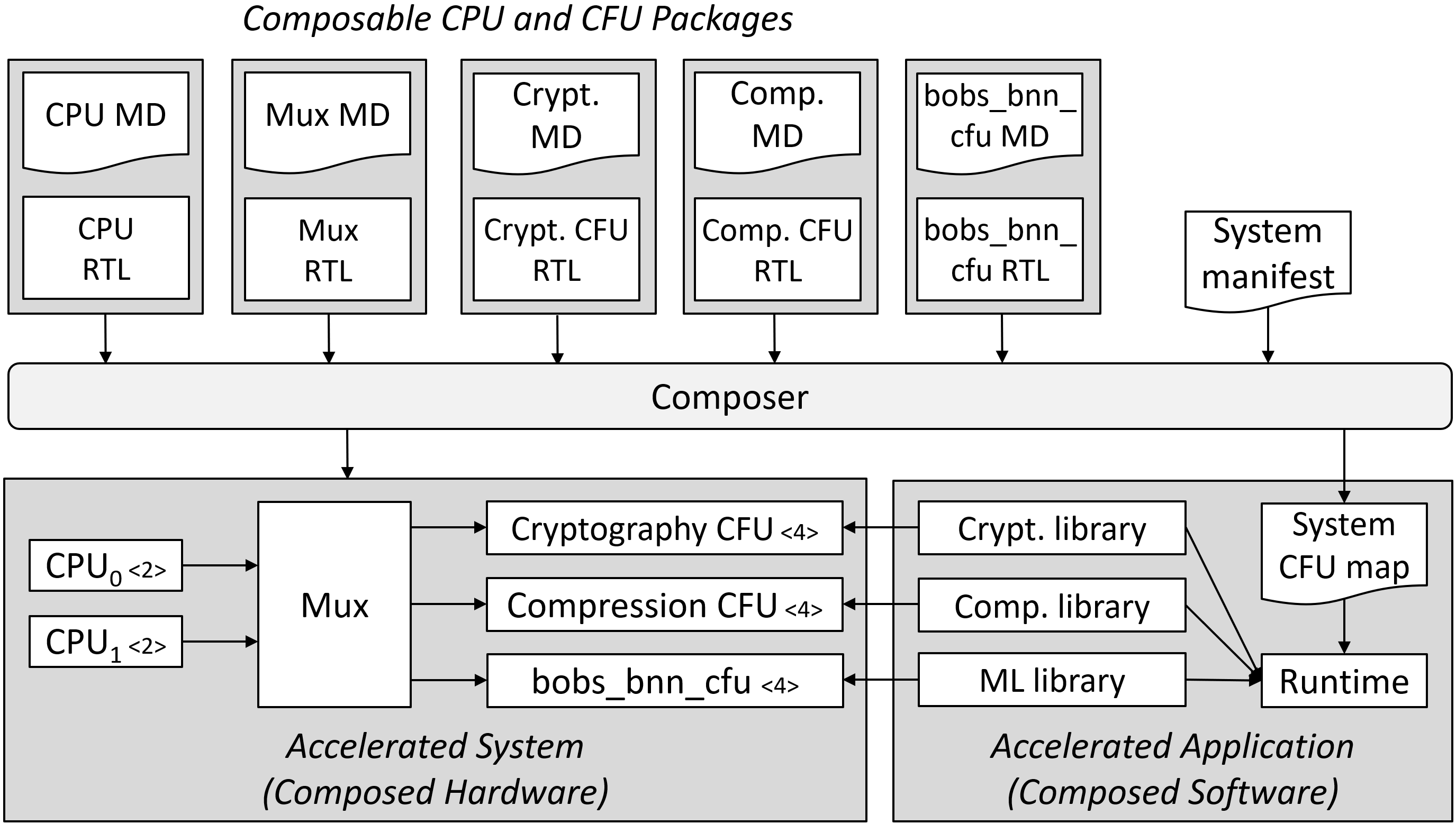
Composing packages of custom interfaces, CPU and CFU cores, and accelerated libraries, into systems
Custom interfaces, their CFUs and libraries, may be open or proprietary, even of narrow interest. Anyone can mint a new one. A new CPU core can use existing CFUs and libraries. A new interface, CFU, or library can be used by existing CPUs and systems. Many CFUs may implement a given custom interface, and many libraries may issue instructions of a custom interface.
Such composition requires routine integration of separately authored, separately versioned elements into stable systems that just work together, now, and over time, as elements evolve. To ensure composition does not change the behavior of any interface, interfaces’ state contexts are isolated: a CF instruction only accesses its source operands and its current state context.
Custom interface multiplexing
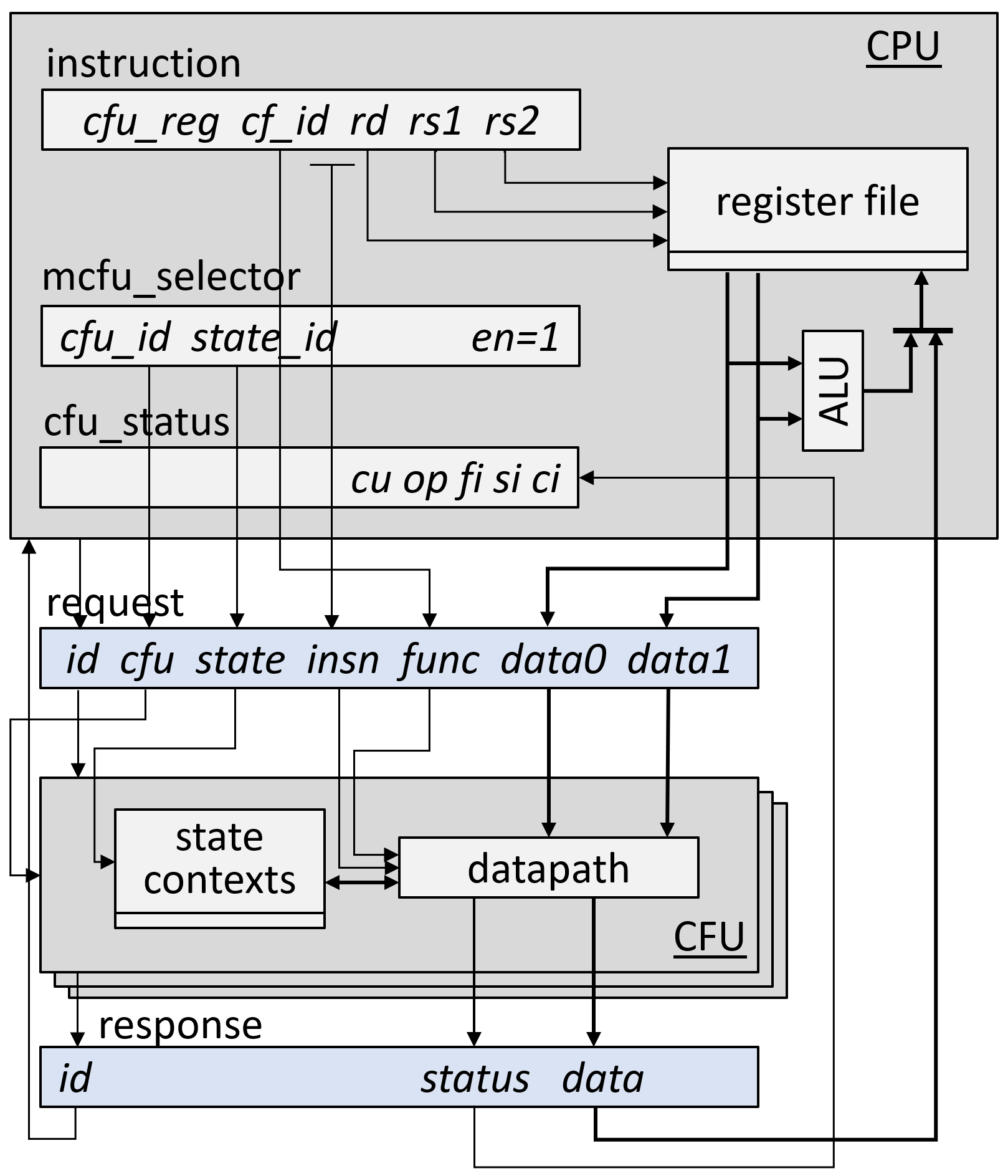
Custom interface multiplexing provides an inexhaustible, collision-free opcode space for custom instructions without any central opcode authority. Every new interface can use any or all of the custom-0/-1 opcode space. Each accelerated CI library, prior to issuing any custom instructions, calls a runtime to obtain that interface’s (CFU,state)selector value and write it to a new mcfu_selector CSR. This selects the hart’s current interface (and CFU core) and its current interface state context. Like the vector extension’s vsetvl instruction, an mcfu_selector write configures the behavior of custom instructions that follow.
HW-SW interface: issuing a custom function instruction using custom interface multiplexing ⇒ CFU logic interface
Custom function unit logic interface (CFU-LI)
A CPU executes a CF instruction by sending a CFU request to a CFU, carrying context IDs and operands. The CFU processes the request, may update its state, and sends a CFU response, which updates a destination register and the cfu_status CSR.
The CFU-LI defines standard signaling and metadata for combinational, fixed-latency, and variable-latency CFUs, so that CPU and CFU packages may be automatically composed.
Example variable-latency, flow controlled CFU-L2 transactions
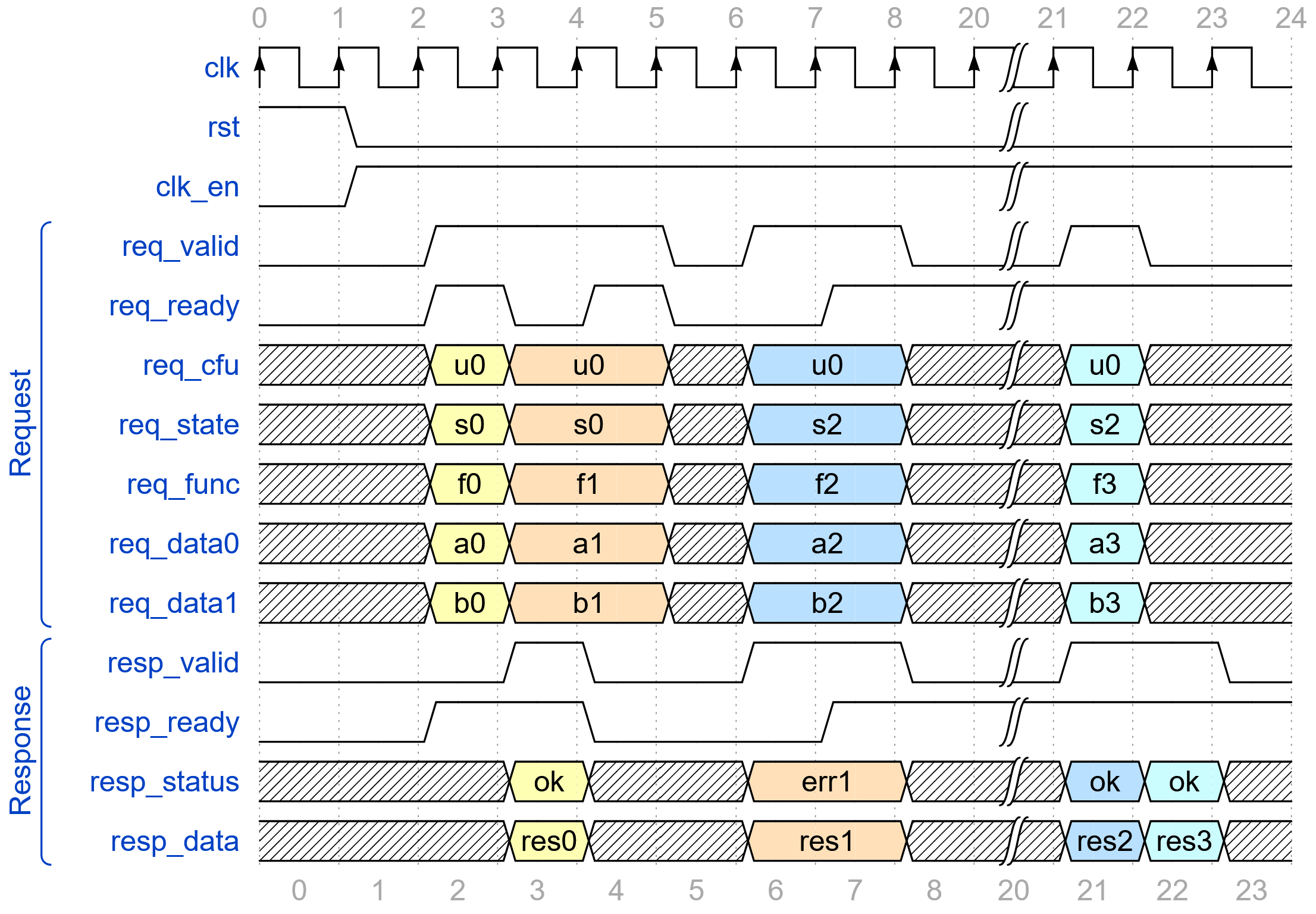
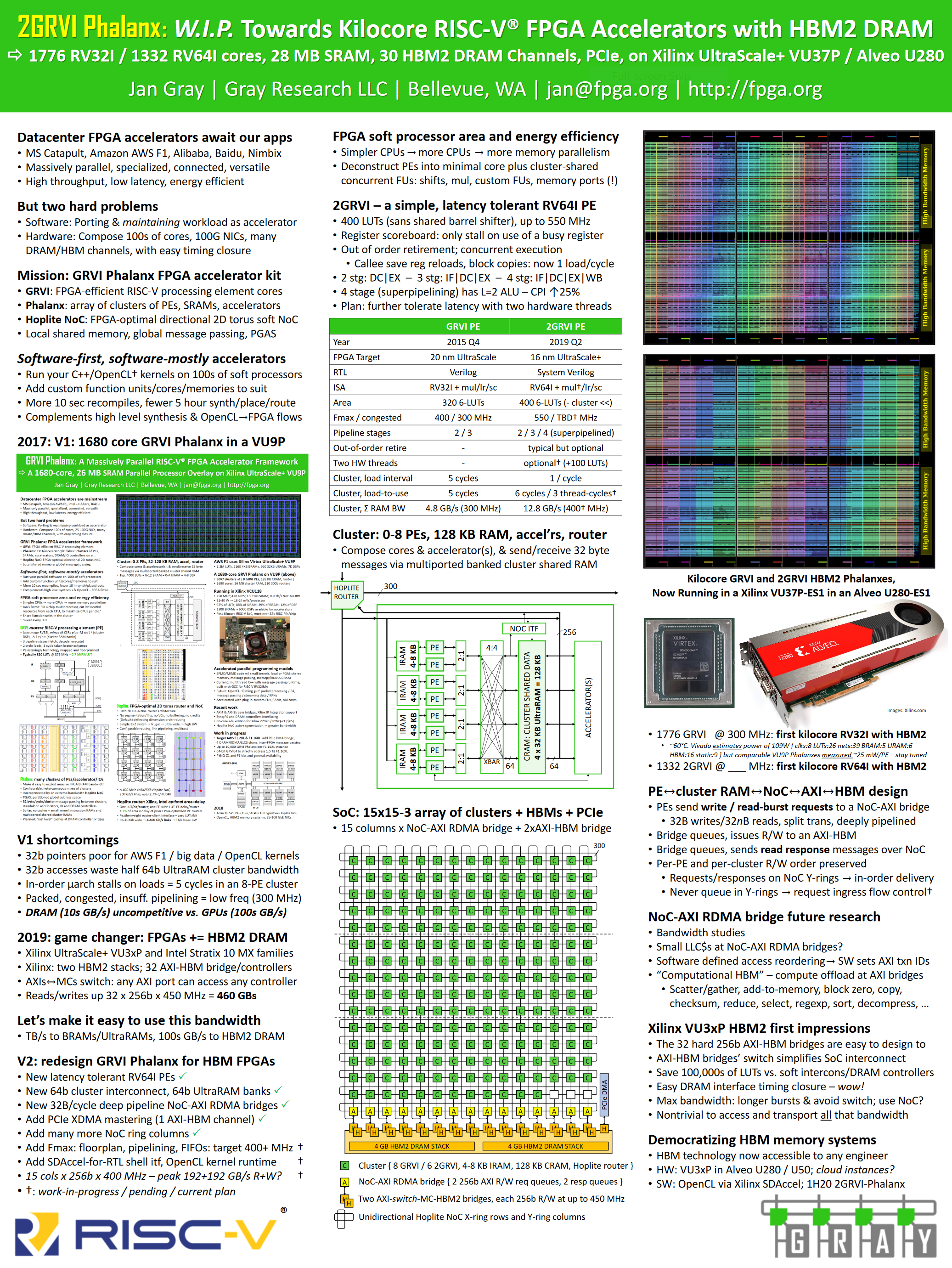
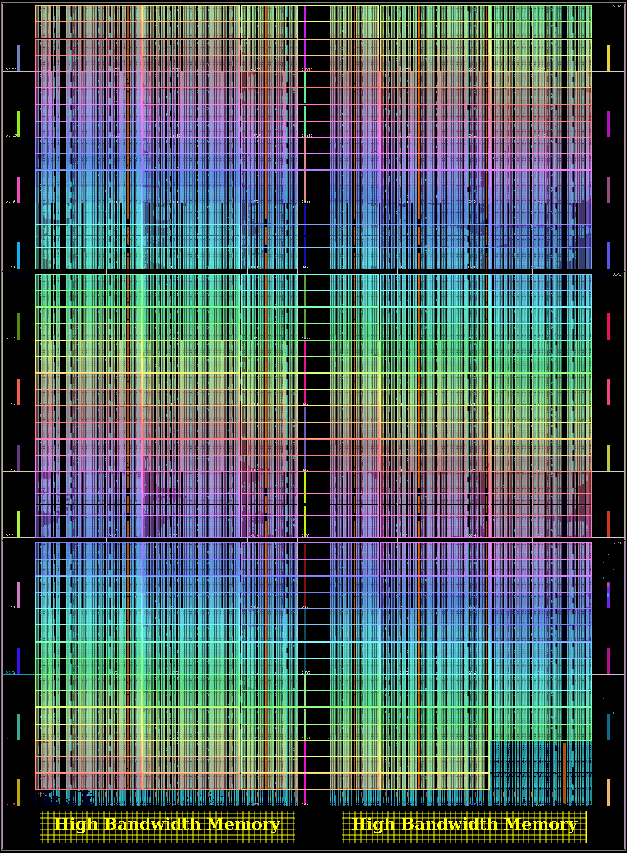
This is the debut of the FPGA-efficient 2GRVI (“too groovy”) RV64I processing element (PE) core, and of Phalanx support for FPGAs with HBM2 high bandwidth DRAM, first discussed last month.
The poster tells the story of the version two redesign of GRVI Phalanx to take best advantage of HBM2 DRAM. It explains some V1 limitations, particularly FPGAs’ relatively low DRAM bandwidth, and shows how the advent of HBM2 FPGAs, such as the Xilinx VCU37P and VU35P in the Alveo U280 and U50 accelerator cards, potentially with over 400 GB/s of memory bandwidth, fundamentally changes the utility and competitiveness of FPGA accelerators.
However, the Niagara of data that 30+ HBM2 memory channels can pour down on your head required changes to the PE and to the Phalanx SoC architecture to request and receive all that sweet sweet bandwidth. These changes include:
New 2GRVI latency-tolerant RV64I PE
New 64b cluster interconnect, 64b UltraRAM banks
New 32B/cycle split transaction pipelined NoC-AXI RDMA bridges
We discuss some of these below, others in another blog post to follow.
New 2GRVI latency-tolerant RV64I 64-bit RISC-V processing element
At just 320 LUTs/PE, the good old 2016-era 32-bit RV32I GRVI PE still has leading soft processor throughput per area. Its frugality made possible the first kilocore 32b RISC processor SoCs, but GRVI’s shortcomings include: 1) its 32-bit address and data width, which is an awkward match to AWS F1’s up to 1.5 TB DRAM, to OpenCL kernels which need to pass 64-bit pointers to global memory buffers, and which wastes half of the bandwidth of 64-bit wide UltraRAM memory banks; 2) its 300-400 MHz Fmax — fast, but not fast enough; and 3) its too-simple scalar RISC microarchitecture, with blocking in-order loads. Blocking loads are fine in a one PE system with a tightly coupled BRAM memory, but in an 8 PE GRVI cluster setting a load can take five cycles there and back through the cluster interconnect to the UltraRAM cluster memory banks (which can be two long trips across one fifth of the width of the die). This is especially painful in a function epilog, reloading n callee save registers, each load taking five cycles. Ugh.
The new RV64I 2GRVI PE tackles these problems: it provides 64-bit addresses and data, up to 550 MHz pipelined execution, and latency tolerance for loads and multi-cycle function units.
Using a busy-register scoreboard, loads do not stall the pipeline until/unless subsequent use of a still busy register — so in a function epilog’s register reloads, or an unrolled block copy loop, 2GRVI issues one load each cycle. The same mechanism enables concurrent execution and out-of-order completion of long latency function units, using a to-be-proposed open Custom Function Unit interface.
As with GRVI, the 64b 2GRVI PE optionally generates RTL obsessively and exquisitely technology mapped for Xilinx 6-LUT FPGAs. It also embraces Jan’s Razor: “In a chip multiprocessor design, strive to leave out all but the minimal kernel set of features from each processing element, so as to maximize processing elements per die.” This leads to a deconstructed PE architecture where functions such as shifts, multiplies, even byte-aligning load/store memory ports, are factored out of the PE core such that multiple PEs share those occasional-use resources. This gets the 64-bit 2GRVI PE core down to just 400 LUTs, and the total area overhead of the PE and its share of a six PE cluster, function units, cluster interconnect, and 300b Hoplite router, is about 700 LUTs.
For its highest Fmax of 550 MHz, 2GRVI can implement a 4-stage pipeline with an initiation interval of one instruction/cycle, but a minimum ALU result latency of two cycles. This enables higher frequency SoC designs, but impairs CPI by 25% or so. To mitigate ALU result-use stalls and four cycle taken branches, I’m also exploring introducing two-way hardware multithreading. This will cost ~100 LUTs, +80 LUTs of which are needed to double the physical register file to 64x64b, so it remains to be seen if this is a net win from the perspective of total throughput / area. We’ll see.
In all, 2GRVI’s XLEN width doubling, load latency tolerance, and higher Fmax means 2GRVI PE clusters have double or triple the total bandwidth to the cluster data RAMs vs. the older GRVI PEs in a GRVI cluster, using the same LUTs and UltraRAMs.
The following table compares and contrasts the two cores.
GRVI
2GRVI
Year
2015 Q4
2019 Q2
FPGA Target
20 nm UltraScale
16 nm UltraScale+
RTL
Verilog
System Verilog
ISA
RV32I + mul* + lr/sc
RV64I + lr/sc (mul WIP) RV32I to come
Area
320 LUTs
400 LUTs (not including barrel shifter)
Fmax / congested
400 / 300 MHz
550 MHz / TBD MHz
Pipeline stages
2 / 3
2 / 3 / 4 (superpipelined)
Latency tolerance: out-of-order retire
–
typical but optional
Latency tolerance: two hardware threads
–
optional (WIP) (+100 LUTs)
Cluster, load initiation interval
5 cycles
1 / cycle
Cluster, load-to-use
5 cycles
6 cycles / 3 thread-cycles (WIP)
Cluster, peak cluster RAM bandwidth
4.8 GB/s (300 MHz)
12.8 GB/s (400 MHz (WIP))
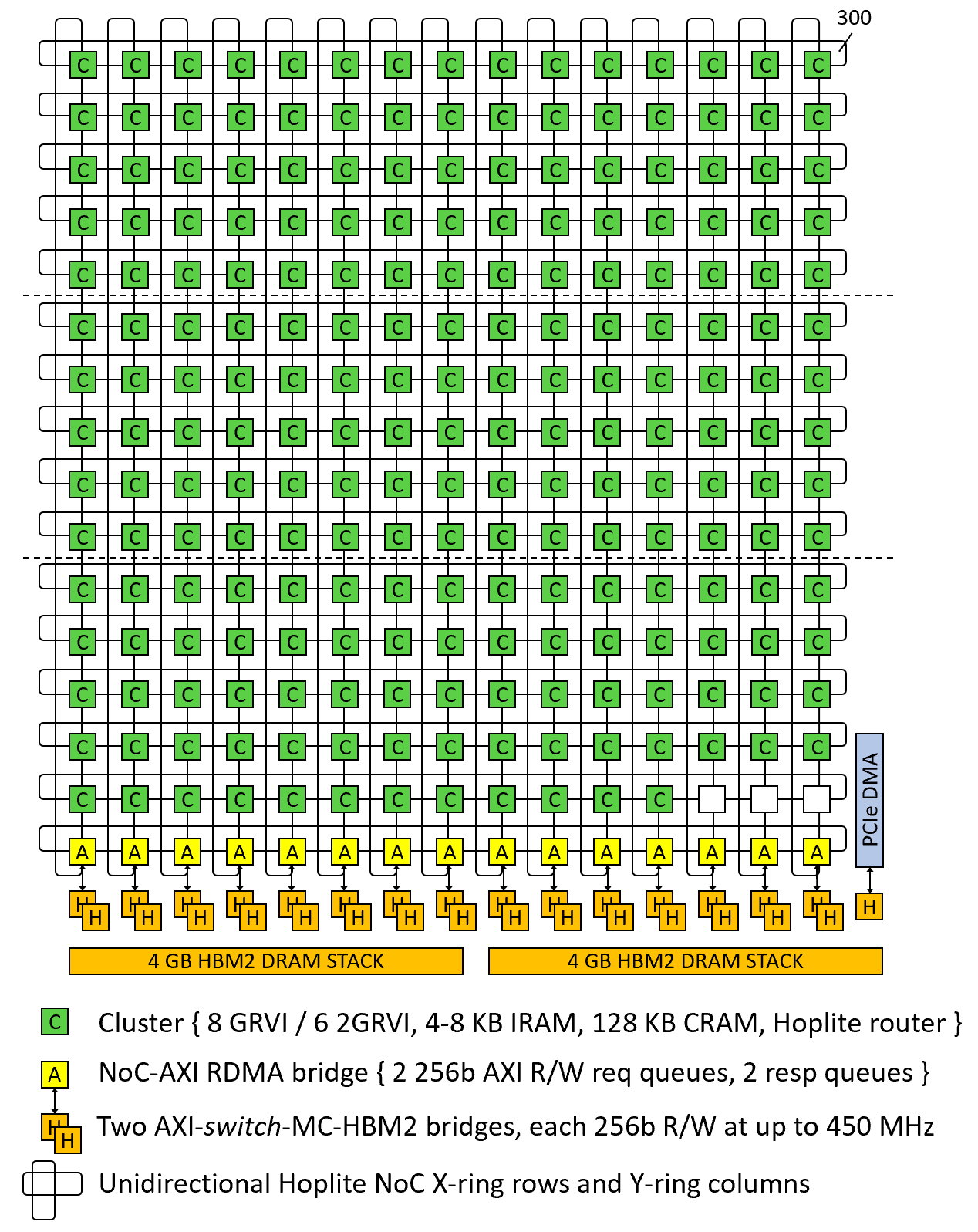
Phalanx redesign for HBM2 memory
The Phalanx “array of clusters, exchanging messages on a NoC” architecture has been redesigned for Xilinx UltraScale+ HBM2 devices such as the VU37P FPGA, with 32 256b @ 450 MHz hardened AXI-HBM controllers coupled to the two stacks (8 GB) of HBM2.
It is rather tricky to move data at up to 3.7 Tb/s to/from the AXI-HBM controllers at the base of the FPGA, from/to the various cores across the length and breadth of the device. A very fast, very wide soft NoC is the way forward, although at FPGA SoC frequencies (300-600 MHz) this requires many thousands of northbound and southbound nets. (The faster the NoC clock, the fewer nets required.)
Then other clock constraints must be considered. The older 32-bit GRVI PEs are too slow; the Hoplite NoC and UltraRAMs can run at 600 MHz, but the AXI-HBM controllers’ Fmax is 450 MHz. To avoid clock domain crossings (for now) we aim to run each component at 450 MHz. (It’s a work-in-progress, we’re not there yet.) Then a 15x15x256b Hoplite NoC will carry ~200 GB/s of read data and ~200 GB/s of write data between the HBM controllers and any FPGA clusters or I/O controllers. While not yet full peak VU37P HBM2 bandwidth, it is nevertheless a giant leap ahead for RISC-V multiprocessors and for FPGA accelerators.
So this redesign depends on three advances: 1) modifying the NoC’s X rings x Y rings topology to include at least twice as many die-spanning vertical Y rings; 2) designing a wide, deeply pipelined NoC-AXI RDMA bridge that can sustain writes and burst reads on back to back clock cycles, 256 bits per bridge per cycle, all day long; and 3) generally increasing the Fmax of every element of the SoC from 300 MHz towards 450 MHz.
At present the first two have been achieved. The 30×7 NoC of the 2017 Hot Chips demonstration is replaced here with a 16×15 NoC with an array of 15×15 PE clusters and a row of 15×1 NoC-AXI RDMA bridges, each coupled to two AXI-HBM bridges. This doubles the NoC bandwidth to the HBM2 bridges. Here’s the new system topology:
The poster presents two different FPGA SoCs design chip plots.
The first is a 1776 PE GRVI Phalanx, with (15×15-3) x 8 32-bit GRVI PEs. (It depopulates three clusters in the bottom right of SLR0, freeing up some LUTs needed for the ~15000 LUT PCIe XDMA logic.)
A 1776 PE GRVI Phalanx, comprising a 15×15-3 array of clusters of eight RISC-V RV32I GRVI PEs, 128 KB cluster RAM, and Hoplite router, plus 15 NoC-AXI RDMA bridges and 30 AXI-HBM bridges.
The second is a 1332 PE 2GRVI Phalanx, with 222 clusters of six 2GRVI RV64I PEs. To our knowledge this is the first operational kilocore 64-bit RISC SoC in any technology, and the first with HBM memory.
A 1332 PE 2GRVI Phalanx, comprising a 15×15-3 array of clusters of six RISC-V RV64I 2GRVI PEs, 128 KB cluster RAM, and Hoplite router, plus 15 NoC-AXI RDMA bridges and 30 AXI-HBM bridges.
A later blog post will drill down into this design, how the memory system works overall, and experiences working with the Xilinx AXI-HBM bridges.
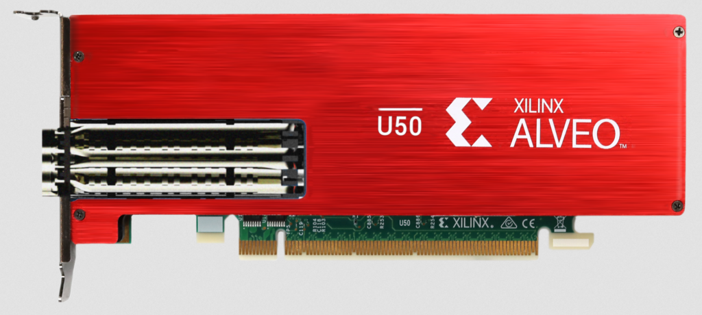
I usually don’t blog about FPGA card announcements but this is a big deal. Finally a vendor FPGA card streamlined and focused on pure data + network compute acceleration, with massive bandwidth (PCIe gen4x8 or gen3x16, QSFP28 for 100 GbE, ~7 TB/s to 5 MB of BRAM, ~6 TB/s to 20 MB of UltraRAM, and 460 GB/s to 8 GB of HBM2 DRAM), in an optimized form factor.
(In particular, it doesn’t have conventional DRAM DIMMs inside, and I think that’s fine. Doesn’t need them, won’t miss them. The key external RAM is the 8 GB of high bandwidth DRAM, right there behind the 32 AXI-HBM controllers. If greater RAM capacity is required, the host has tens or hundreds of GB that can be streamed in/out across PCIe. And no more sprawling soft DDR4 DRAM controllers in your design.)
Now FPGA uptake as mainstream data center accelerator platforms really depends upon their performance and cost competitiveness vs. multicore CPUs and GPUs. GPUs, with GDDRx and HBM2 DRAM memory systems, have always enjoyed a big lead in peak external memory bandwidth vs. FPGAs. This advantage has limited the types of workloads for which FPGAs are faster, or at least performance competitive. But the advent of Xilinx Virtex UltraScale+ VU3xP and Intel Stratix 10 MX devices, with HBM2 DRAM in package, now give FPGAs CPU-beating, GPU-competitive memory bandwidth. The next frontier is cost. So far, HBM2-powered FPGA cards have been expensive, many times more expensive than a GPU card with comparable bandwidth. I hope U50 will move the needle on price competitiveness, a prerequisite for FPGA accelerators to reach high volume economies of scale and support a thriving solution provider ecosystem.
Under the hood
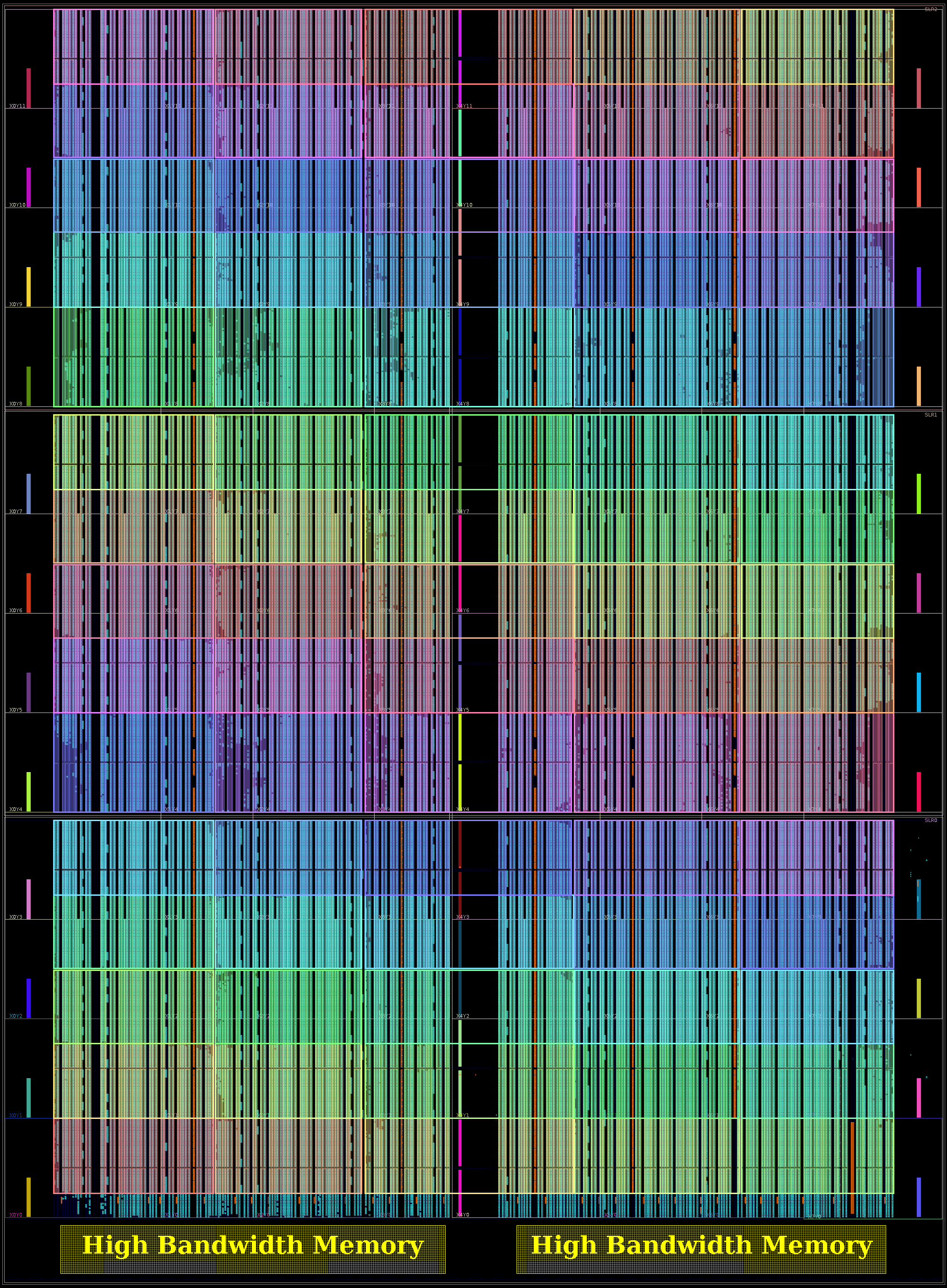
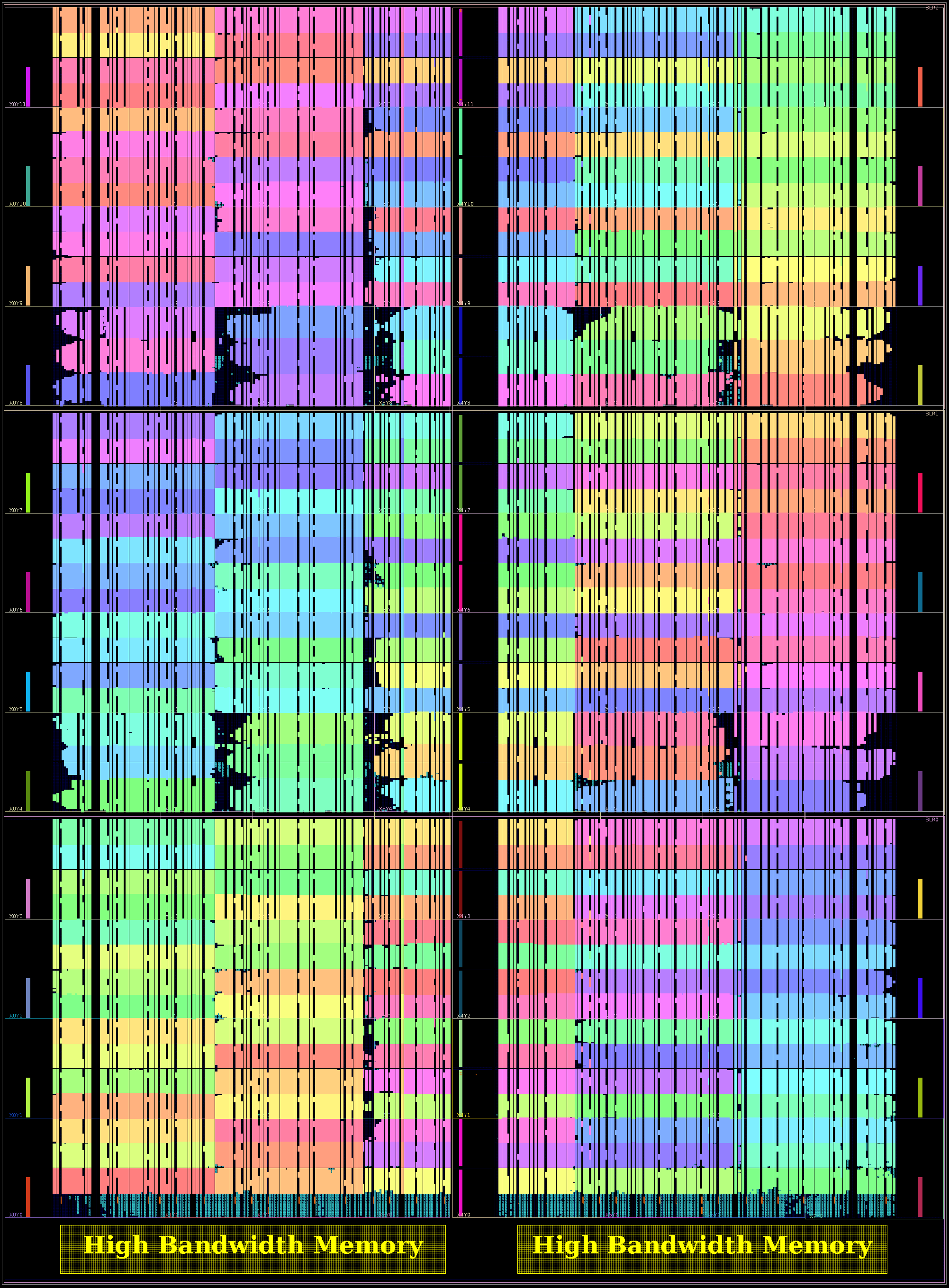
The User Guide and Data Sheet describes the FPGA as an UltraScale+ XCU50, with 872K 6-LUTs, 5952 DSPs, 1344 BRAMs, 640 UltraRAMs, and two stacks of 4 GB HBM2 DRAM. While the XCU50 is not in the UltraScale+ Product Tables, these resources exactly match that of the XCVU35P, as does this floorplan figure:
XCU50 FPGA floorplan
Assuming this is the same silicon as the VU35P, that’s fantastic news — this part is extremely capable. For example, here is another kilocore RISC-V GRVI Phalanx with HBM2, for VU35P:
An 1176 RISC-V PE implementation of the GRVI Phalanx massively parallel accelerator framework in a VU35P. 10×15 -3 clusters of { 8 PE, 128 KB SRAM, 300b Hoplite NoC router }, 30 HBM DRAM channels, PCIe DMA controller.
I look forward to an exciting future of mainstream FPGA+HBM2 accelerator cards, as common as GPU accelerator cards, deployed across the industry, there and just waiting for all of our problems, ingenuity, workloads, and bitstreams. Today’s Alveo U50 launch is a big milestone in this march to the mainstream. Congratulations to Xilinx, its staff, and partners.
A kilocore processor with a few DDR4 DRAM channels has never made much sense, and so today I am happy to announce that the GRVI Phalanx massively parallel RISC-V accelerator framework is now running on a Xilinx UltraScale+ VU37P FPGA with 8 GB of integrated in-package HBM2 DRAM, on a Xilinx Alveo U280 accelerator card.
This new FPGA SoC overlay is configured with a 15×15 array of clusters of 8 GRVI RISC-V PEs, 128 KB of SRAM, and a 300b Hoplite NoC router. In total it has 1800 PEs, 28 MB of SRAM, 8 GB of HBM2, 240 Hoplite NoC routers, 30 256b Hoplite-AXI RDMA bridges, and 31 AXI-HBM channels.
An 1800 RISC-V PE implementation of the GRVI Phalanx massively parallel accelerator framework. 15×15 clusters of { 8 PE, 128 KB SRAM, 300b Hoplite NoC router }.
We’ll have more to say about this new design in the coming weeks. Thank you for your interest.
![Excerpt of %5.1 of the spec, illustrating an MX format block with one shared scale X and k scalar elements P[].](https://fpga.org/wp-content/uploads/2023/10/image.png)