Category Archives: NOCs

2GRVI Phalanx at Hot Chips 31 (2019): The First Kilocore RISC-V RV64I with High Bandwidth Memory

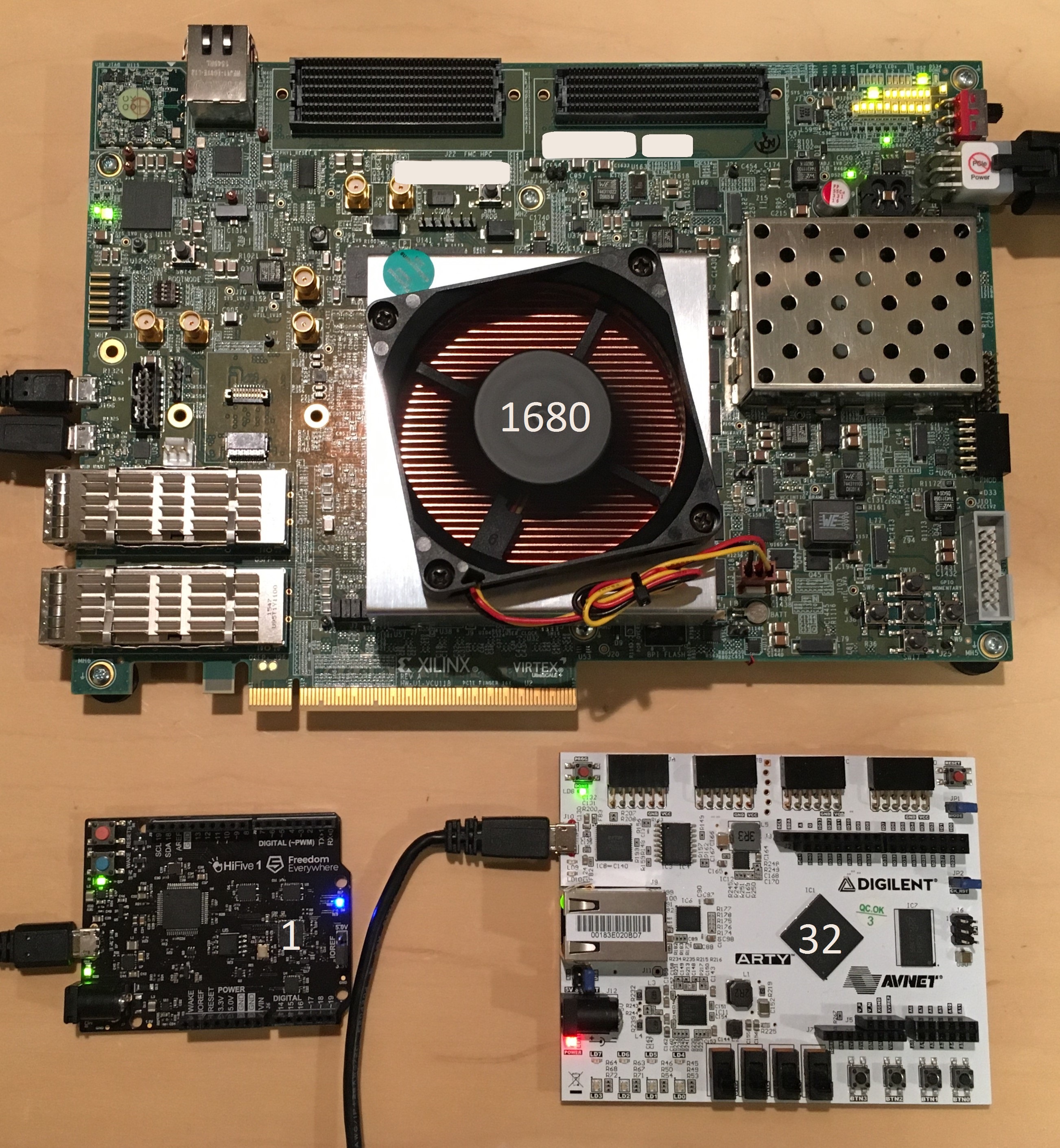
This week at Hot Chips 31 (2019) I am presenting a status update poster on the work-in-progress GRVI Phalanx Accelerator Kit: 2GRVI Phalanx: Towards Kilocore RISC-V FPGA Accelerators with HBM2 DRAM (PDF).

This is the debut of the FPGA-efficient 2GRVI (“too groovy”) RV64I processing element (PE) core, and of Phalanx support for FPGAs with HBM2 high bandwidth DRAM, first discussed last month.

The poster tells the story of the version two redesign of GRVI Phalanx to take best advantage of HBM2 DRAM. It explains some V1 limitations, particularly FPGAs’ relatively low DRAM bandwidth, and shows how the advent of HBM2 FPGAs, such as the Xilinx VCU37P and VU35P in the Alveo U280 and U50 accelerator cards, potentially with over 400 GB/s of memory bandwidth, fundamentally changes the utility and competitiveness of FPGA accelerators.

However, the Niagara of data that 30+ HBM2 memory channels can pour down on your head required changes to the PE and to the Phalanx SoC architecture to request and receive all that sweet sweet bandwidth. These changes include:

  • New 2GRVI latency-tolerant RV64I PE
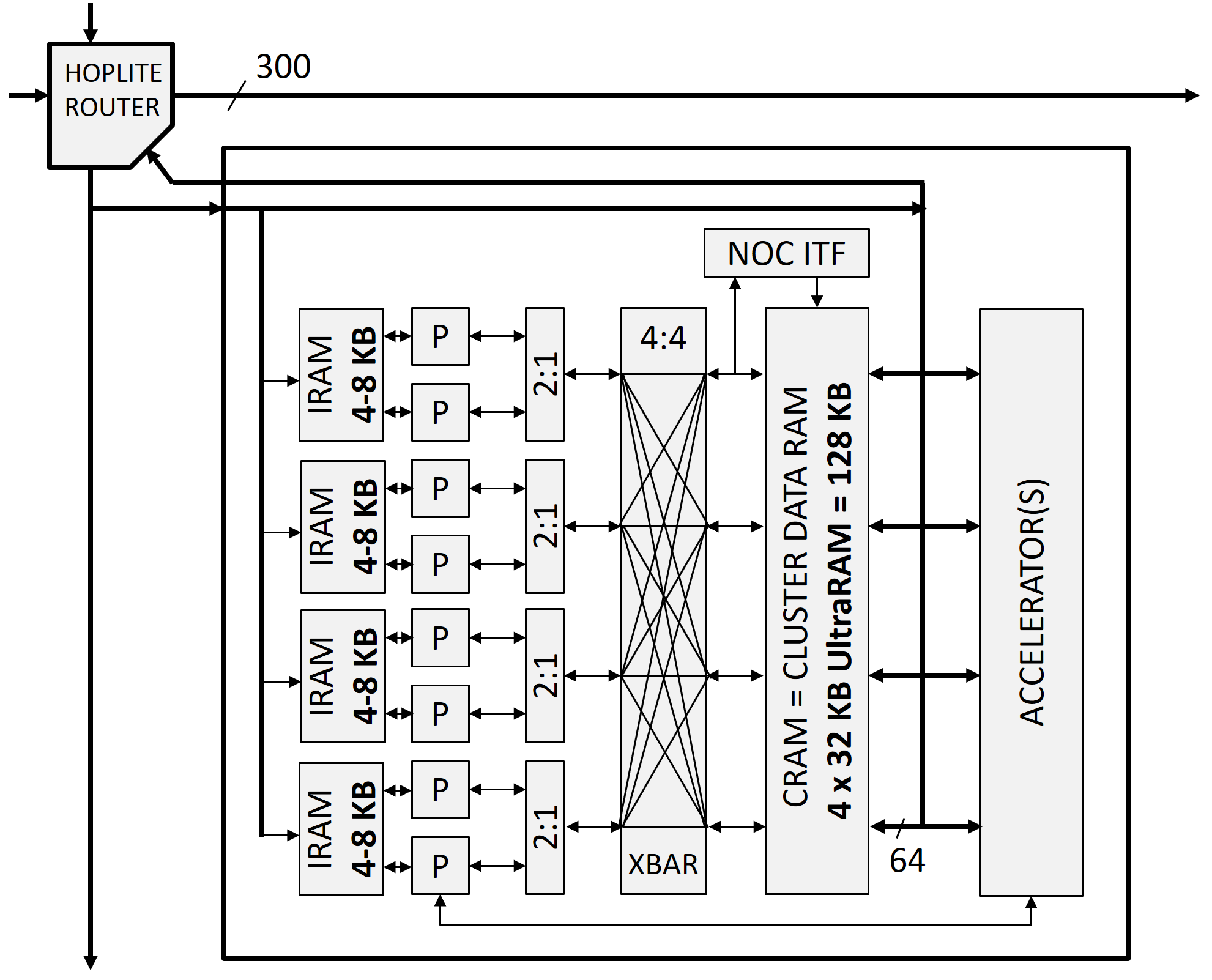
  • New 64b cluster interconnect, 64b UltraRAM banks
  • New 32B/cycle split transaction pipelined NoC-AXI RDMA bridges
  • Add PCIe XDMA mastering (to an AXI-HBM channel)
  • Add many more Hoplite NoC ring columns

We discuss some of these below, others in another blog post to follow.

New 2GRVI latency-tolerant RV64I 64-bit RISC-V processing element

At just 320 LUTs/PE, the good old 2016-era 32-bit RV32I GRVI PE still has leading soft processor throughput per area. Its frugality made possible the first kilocore 32b RISC processor SoCs, but GRVI’s shortcomings include: 1) its 32-bit address and data width, which is an awkward match to AWS F1’s up to 1.5 TB DRAM, to OpenCL kernels which need to pass 64-bit pointers to global memory buffers, and which wastes half of the bandwidth of 64-bit wide UltraRAM memory banks; 2) its 300-400 MHz Fmax — fast, but not fast enough; and 3) its too-simple scalar RISC microarchitecture, with blocking in-order loads. Blocking loads are fine in a one PE system with a tightly coupled BRAM memory, but in an 8 PE GRVI cluster setting a load can take five cycles there and back through the cluster interconnect to the UltraRAM cluster memory banks (which can be two long trips across one fifth of the width of the die). This is especially painful in a function epilog, reloading n callee save registers, each load taking five cycles. Ugh.

The new RV64I 2GRVI PE tackles these problems: it provides 64-bit addresses and data, up to 550 MHz pipelined execution, and latency tolerance for loads and multi-cycle function units.

Using a busy-register scoreboard, loads do not stall the pipeline until/unless subsequent use of a still busy register — so in a function epilog’s register reloads, or an unrolled block copy loop, 2GRVI issues one load each cycle. The same mechanism enables concurrent execution and out-of-order completion of long latency function units, using a to-be-proposed open Custom Function Unit interface.

As with GRVI, the 64b 2GRVI PE optionally generates RTL obsessively and exquisitely technology mapped for Xilinx 6-LUT FPGAs. It also embraces Jan’s Razor: “In a chip multiprocessor design, strive to leave out all but the minimal kernel set of features from each processing element, so as to maximize processing elements per die.” This leads to a deconstructed PE architecture where functions such as shifts, multiplies, even byte-aligning load/store memory ports, are factored out of the PE core such that multiple PEs share those occasional-use resources. This gets the 64-bit 2GRVI PE core down to just 400 LUTs, and the total area overhead of the PE and its share of a six PE cluster, function units, cluster interconnect, and 300b Hoplite router, is about 700 LUTs.

For its highest Fmax of 550 MHz, 2GRVI can implement a 4-stage pipeline with an initiation interval of one instruction/cycle, but a minimum ALU result latency of two cycles. This enables higher frequency SoC designs, but impairs CPI by 25% or so. To mitigate ALU result-use stalls and four cycle taken branches, I’m also exploring introducing two-way hardware multithreading. This will cost ~100 LUTs, +80 LUTs of which are needed to double the physical register file to 64x64b, so it remains to be seen if this is a net win from the perspective of total throughput / area. We’ll see.

In all, 2GRVI’s XLEN width doubling, load latency tolerance, and higher Fmax means 2GRVI PE clusters have double or triple the total bandwidth to the cluster data RAMs vs. the older GRVI PEs in a GRVI cluster, using the same LUTs and UltraRAMs.

The following table compares and contrasts the two cores.

GRVI2GRVI
Year2015 Q42019 Q2
FPGA Target20 nm UltraScale16 nm UltraScale+
RTLVerilogSystem Verilog
ISARV32I + mul* + lr/scRV64I + lr/sc (mul WIP)
RV32I to come
Area320 LUTs400 LUTs (not including barrel shifter)
Fmax / congested400 / 300 MHz550 MHz / TBD MHz
Pipeline stages2 / 32 / 3 / 4 (superpipelined)
Latency tolerance: out-of-order retiretypical but optional
Latency tolerance: two hardware threadsoptional (WIP) (+100 LUTs)
Cluster, load initiation interval5 cycles1 / cycle
Cluster, load-to-use5 cycles6 cycles / 3 thread-cycles (WIP)
Cluster, peak cluster RAM bandwidth4.8 GB/s (300 MHz)12.8 GB/s (400 MHz (WIP))

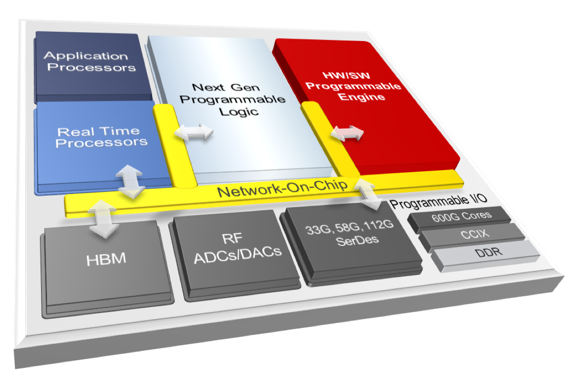
Phalanx redesign for HBM2 memory

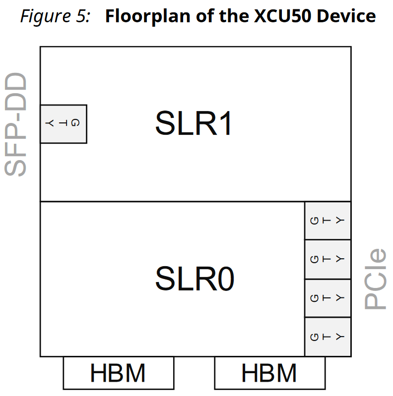
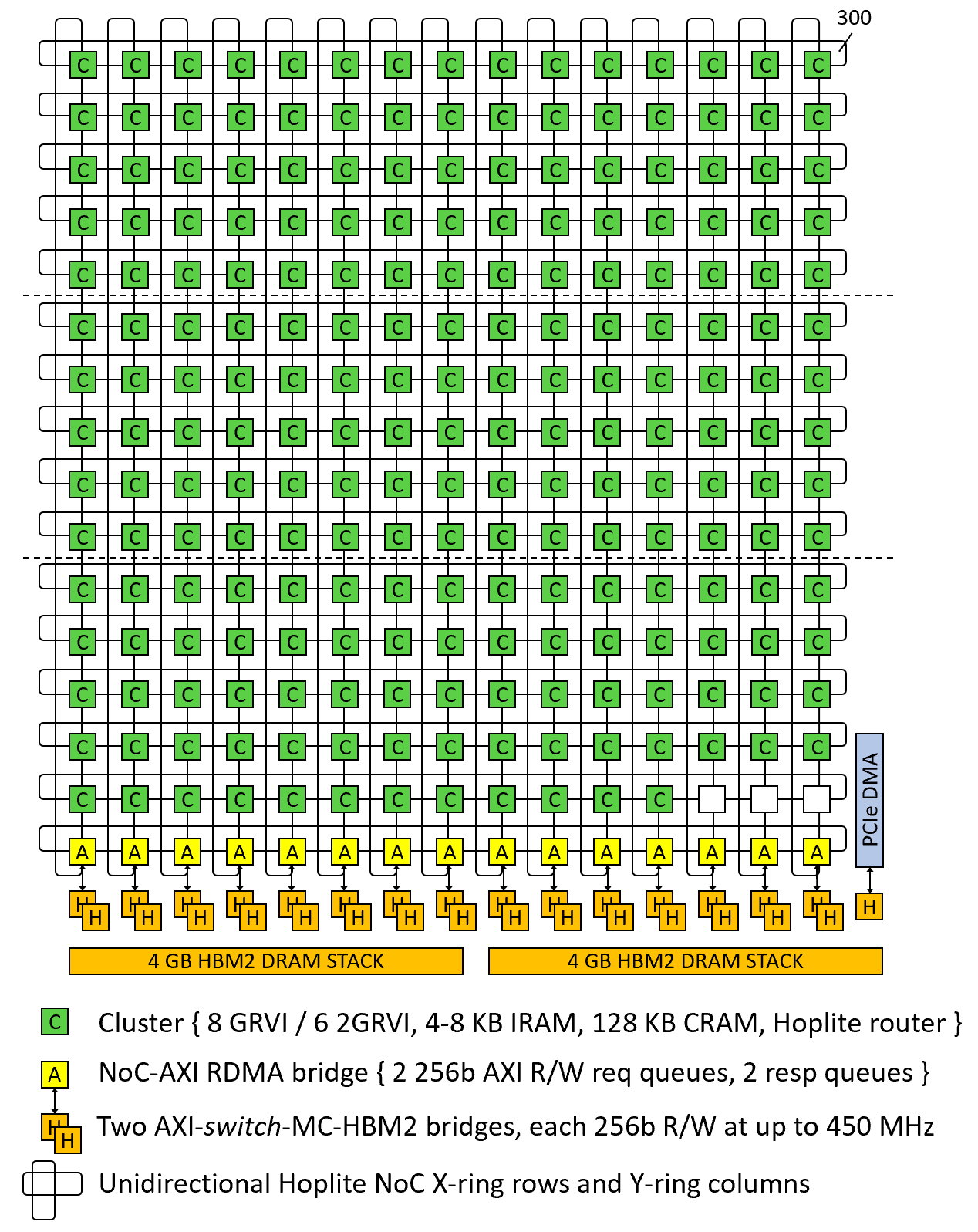
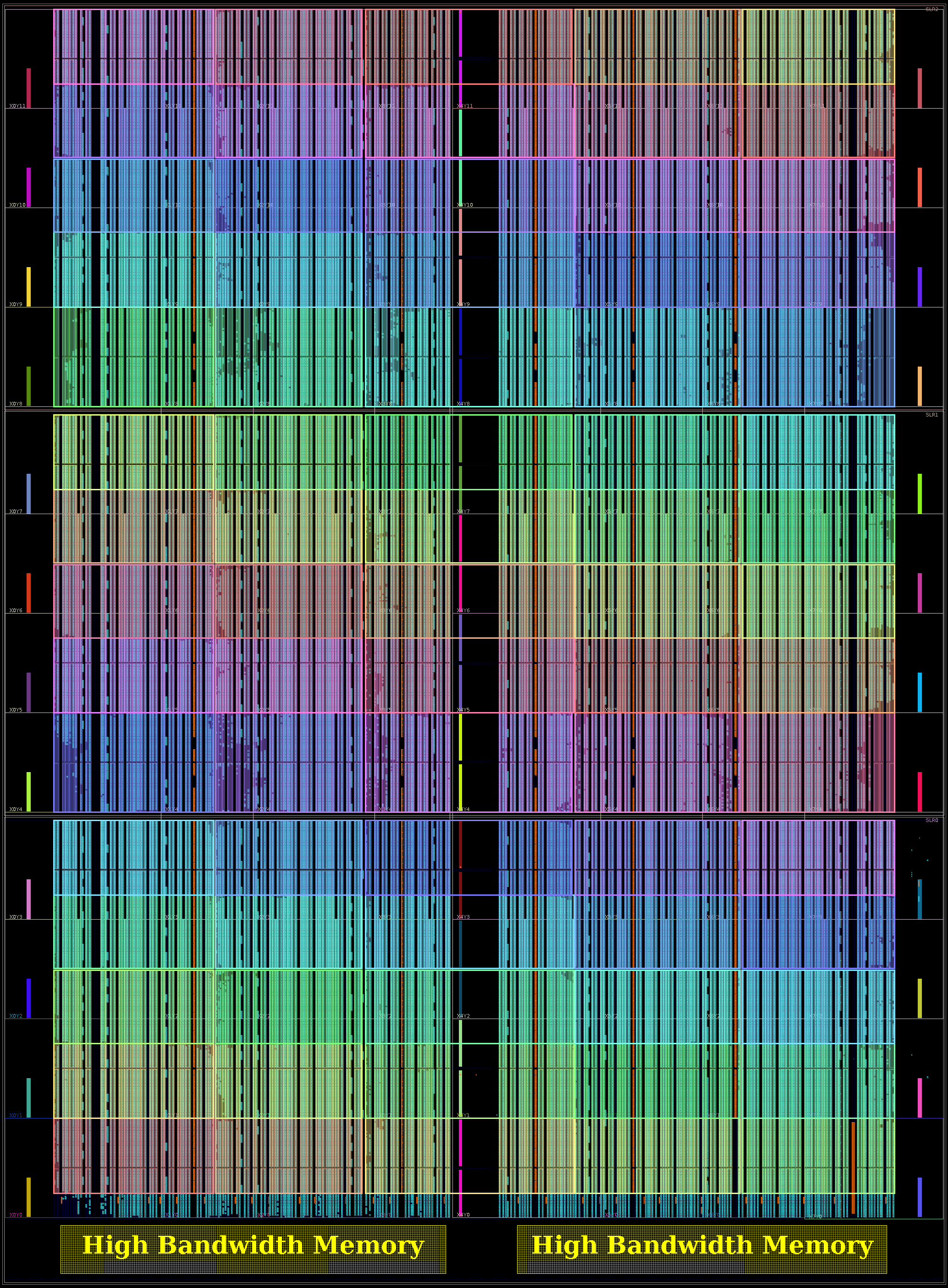
The Phalanx “array of clusters, exchanging messages on a NoC” architecture has been redesigned for Xilinx UltraScale+ HBM2 devices such as the VU37P FPGA, with 32 256b @ 450 MHz hardened AXI-HBM controllers coupled to the two stacks (8 GB) of HBM2.

It is rather tricky to move data at up to 3.7 Tb/s to/from the AXI-HBM controllers at the base of the FPGA, from/to the various cores across the length and breadth of the device. A very fast, very wide soft NoC is the way forward, although at FPGA SoC frequencies (300-600 MHz) this requires many thousands of northbound and southbound nets. (The faster the NoC clock, the fewer nets required.)

Then other clock constraints must be considered. The older 32-bit GRVI PEs are too slow; the Hoplite NoC and UltraRAMs can run at 600 MHz, but the AXI-HBM controllers’ Fmax is 450 MHz. To avoid clock domain crossings (for now) we aim to run each component at 450 MHz. (It’s a work-in-progress, we’re not there yet.) Then a 15x15x256b Hoplite NoC will carry ~200 GB/s of read data and ~200 GB/s of write data between the HBM controllers and any FPGA clusters or I/O controllers. While not yet full peak VU37P HBM2 bandwidth, it is nevertheless a giant leap ahead for RISC-V multiprocessors and for FPGA accelerators.

So this redesign depends on three advances: 1) modifying the NoC’s X rings x Y rings topology to include at least twice as many die-spanning vertical Y rings; 2) designing a wide, deeply pipelined NoC-AXI RDMA bridge that can sustain writes and burst reads on back to back clock cycles, 256 bits per bridge per cycle, all day long; and 3) generally increasing the Fmax of every element of the SoC from 300 MHz towards 450 MHz.

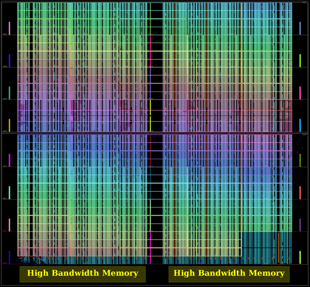
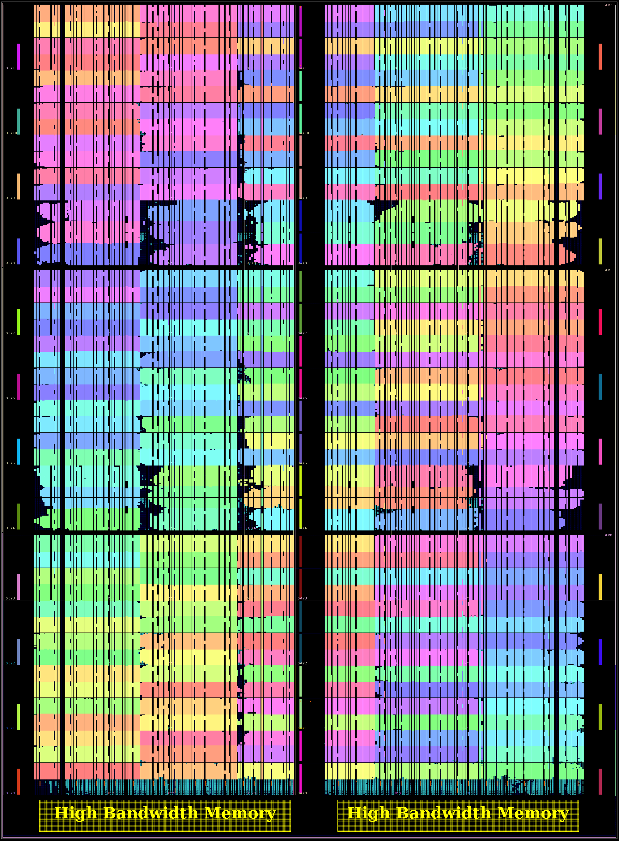
At present the first two have been achieved. The 30×7 NoC of the 2017 Hot Chips demonstration is replaced here with a 16×15 NoC with an array of 15×15 PE clusters and a row of 15×1 NoC-AXI RDMA bridges, each coupled to two AXI-HBM bridges. This doubles the NoC bandwidth to the HBM2 bridges. Here’s the new system topology:

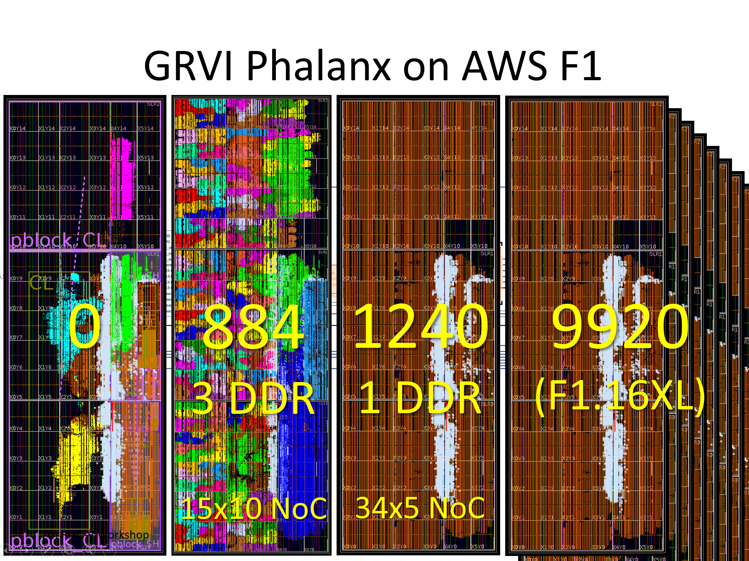
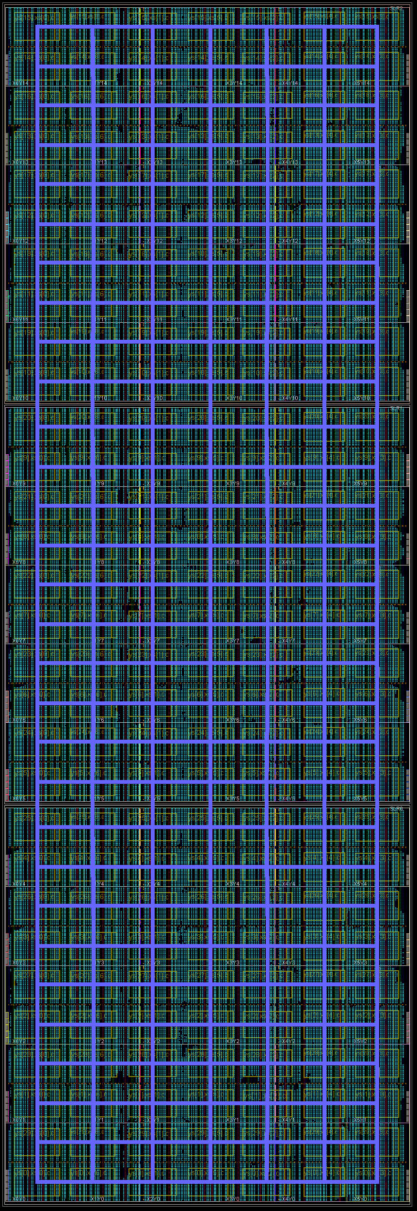
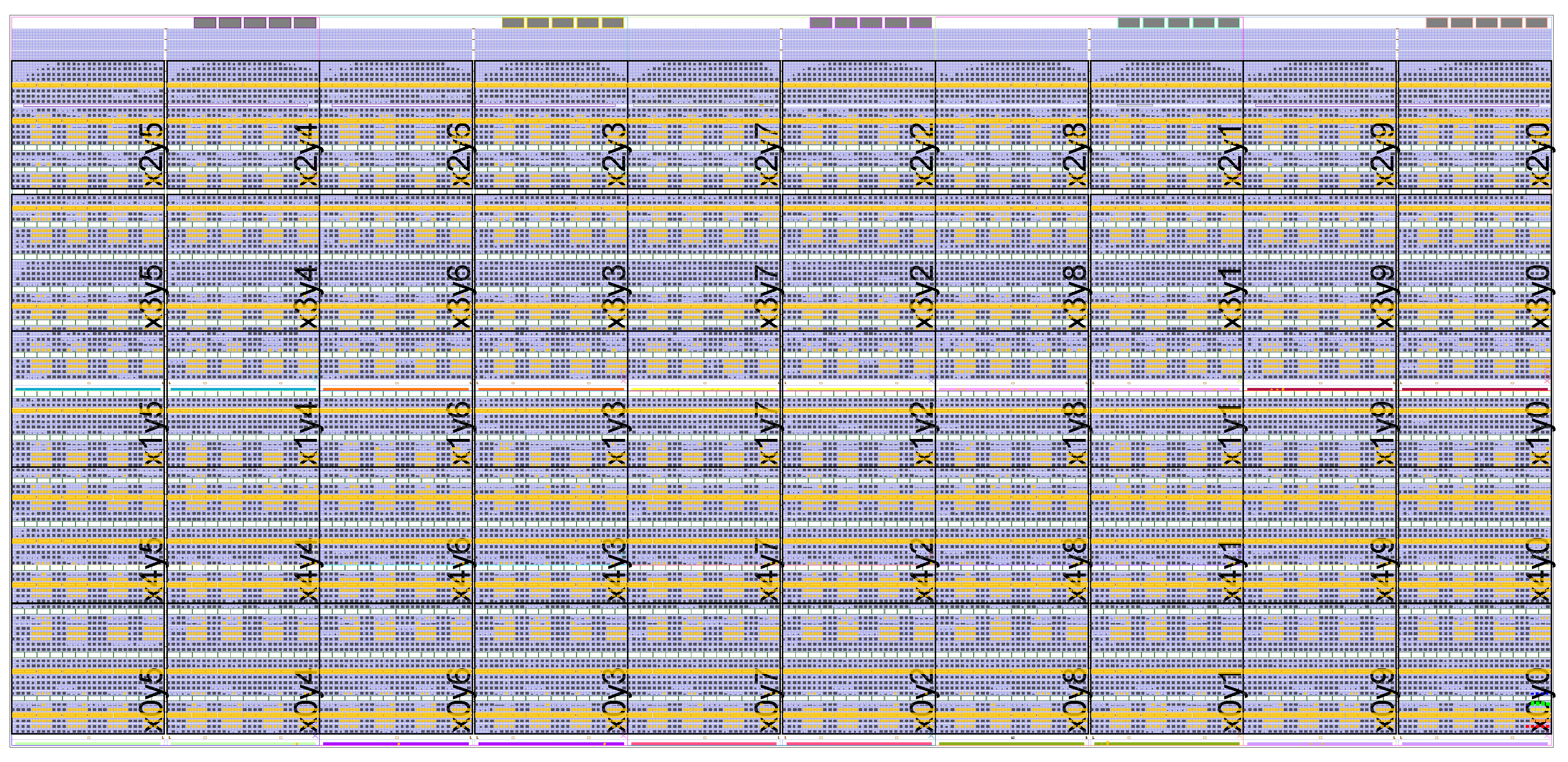
The poster presents two different FPGA SoCs design chip plots.

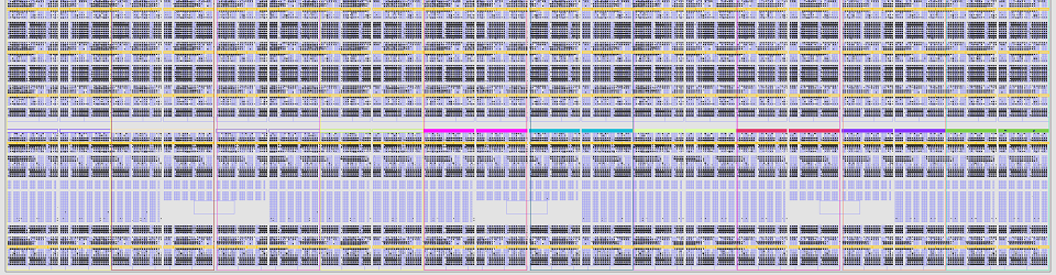
The first is a 1776 PE GRVI Phalanx, with (15×15-3) x 8 32-bit GRVI PEs. (It depopulates three clusters in the bottom right of SLR0, freeing up some LUTs needed for the ~15000 LUT PCIe XDMA logic.)

A 1776 PE GRVI Phalanx, comprising a 15×15-3 array of clusters of eight RISC-V RV32I GRVI PEs, 128 KB cluster RAM, and Hoplite router, plus 15 NoC-AXI RDMA bridges and 30 AXI-HBM bridges.

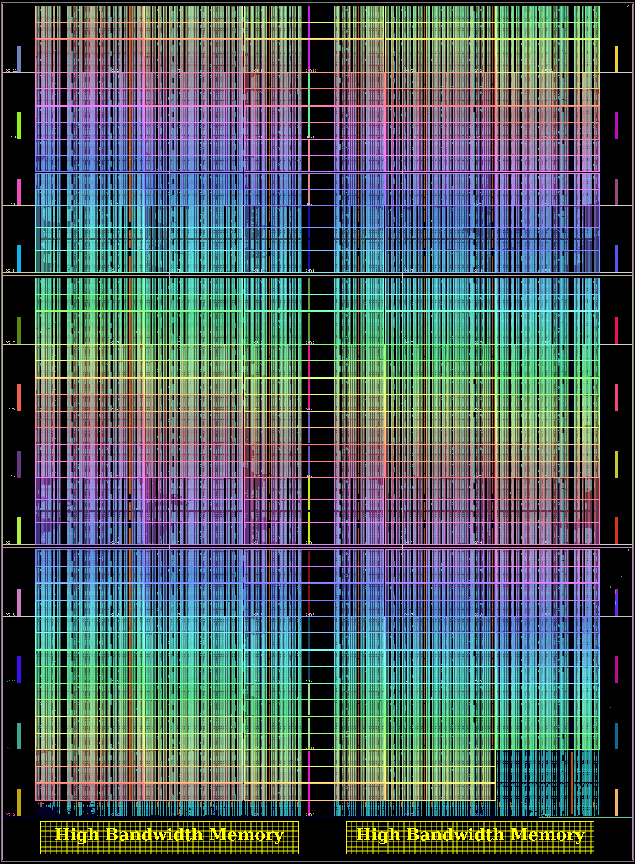
The second is a 1332 PE 2GRVI Phalanx, with 222 clusters of six 2GRVI RV64I PEs. To our knowledge this is the first operational kilocore 64-bit RISC SoC in any technology, and the first with HBM memory.

A 1332 PE 2GRVI Phalanx, comprising a 15×15-3 array of clusters of six RISC-V RV64I 2GRVI PEs, 128 KB cluster RAM, and Hoplite router, plus 15 NoC-AXI RDMA bridges and 30 AXI-HBM bridges.

A later blog post will drill down into this design, how the memory system works overall, and experiences working with the Xilinx AXI-HBM bridges.

Welcome Xilinx Alveo U50!

Today Xilinx announced the new Alveo U50 Data Center Accelerator Card. Press release. Launch presentation. U50 Home. Product Brief. Data Sheet. User Guide.

I usually don’t blog about FPGA card announcements but this is a big deal. Finally a vendor FPGA card streamlined and focused on pure data + network compute acceleration, with massive bandwidth (PCIe gen4x8 or gen3x16, QSFP28 for 100 GbE, ~7 TB/s to 5 MB of BRAM, ~6 TB/s to 20 MB of UltraRAM, and 460 GB/s to 8 GB of HBM2 DRAM), in an optimized form factor.

(In particular, it doesn’t have conventional DRAM DIMMs inside, and I think that’s fine. Doesn’t need them, won’t miss them. The key external RAM is the 8 GB of high bandwidth DRAM, right there behind the 32 AXI-HBM controllers. If greater RAM capacity is required, the host has tens or hundreds of GB that can be streamed in/out across PCIe. And no more sprawling soft DDR4 DRAM controllers in your design.)

Now FPGA uptake as mainstream data center accelerator platforms really depends upon their performance and cost competitiveness vs. multicore CPUs and GPUs. GPUs, with GDDRx and HBM2 DRAM memory systems, have always enjoyed a big lead in peak external memory bandwidth vs. FPGAs. This advantage has limited the types of workloads for which FPGAs are faster, or at least performance competitive. But the advent of Xilinx Virtex UltraScale+ VU3xP and Intel Stratix 10 MX devices, with HBM2 DRAM in package, now give FPGAs CPU-beating, GPU-competitive memory bandwidth. The next frontier is cost. So far, HBM2-powered FPGA cards have been expensive, many times more expensive than a GPU card with comparable bandwidth. I hope U50 will move the needle on price competitiveness, a prerequisite for FPGA accelerators to reach high volume economies of scale and support a thriving solution provider ecosystem.

Under the hood

The User Guide and Data Sheet describes the FPGA as an UltraScale+ XCU50, with 872K 6-LUTs, 5952 DSPs, 1344 BRAMs, 640 UltraRAMs, and two stacks of 4 GB HBM2 DRAM. While the XCU50 is not in the UltraScale+ Product Tables, these resources exactly match that of the XCVU35P, as does this floorplan figure:

XCU50 FPGA floorplan

Assuming this is the same silicon as the VU35P, that’s fantastic news — this part is extremely capable. For example, here is another kilocore RISC-V GRVI Phalanx with HBM2, for VU35P:

1176 RISC-V PE GRVI Phalanx with 30 HBM DRAM channels
An 1176 RISC-V PE implementation of the GRVI Phalanx massively parallel accelerator framework in a VU35P.
10×15 -3 clusters of { 8 PE, 128 KB SRAM, 300b Hoplite NoC router }, 30 HBM DRAM channels, PCIe DMA controller.

I look forward to an exciting future of mainstream FPGA+HBM2 accelerator cards, as common as GPU accelerator cards, deployed across the industry, there and just waiting for all of our problems, ingenuity, workloads, and bitstreams. Today’s Alveo U50 launch is a big milestone in this march to the mainstream. Congratulations to Xilinx, its staff, and partners.

GRVI Phalanx: The First Kilocore RISC-V with High Bandwidth Memory

A kilocore processor with a few DDR4 DRAM channels has never made much sense, and so today I am happy to announce that the GRVI Phalanx massively parallel RISC-V accelerator framework is now running on a Xilinx UltraScale+ VU37P FPGA with 8 GB of integrated in-package HBM2 DRAM, on a Xilinx Alveo U280 accelerator card.

This new FPGA SoC overlay is configured with a 15×15 array of clusters of 8 GRVI RISC-V PEs, 128 KB of SRAM, and a 300b Hoplite NoC router. In total it has 1800 PEs, 28 MB of SRAM, 8 GB of HBM2, 240 Hoplite NoC routers, 30 256b Hoplite-AXI RDMA bridges, and 31 AXI-HBM channels.

An FPGA device view (chip plot) of an 1800 RISC-V PE implementation of the GRVI Phalanx massively parallel accelerator framework.
15x15 clusters of { 8 PE, 128 KB SRAM, and a 300b Hoplite NoC router }. The die plot consists of 45 rows of 5 columns of variously colored regions, with two High Bandwidth Memory die stacks at the bottom.
An 1800 RISC-V PE implementation of the GRVI Phalanx massively parallel accelerator framework.
15×15 clusters of { 8 PE, 128 KB SRAM, 300b Hoplite NoC router }.

We’ll have more to say about this new design in the coming weeks. Thank you for your interest.

Welcome Xilinx Project Everest

Xilinx Everest block diagram

Everest: A New Adaptive Compute Acceleration Stack

Start with this Xilinx presentation from Victor Peng, Xilinx CEO: Xilinx Vision and Strategy for the Adapatable World. (Dear Xilinx: please share a recording of this presentation.)

Blog and press roundup:

My take: Everest is bold bet on Xilinx’s “data center first” strategy. I see Everest as Xilinx’s response to the present situation that its FPGAs beat GPUs on energy efficiency and integrated data center networking, but not raw compute, and they significantly trail CPUs and GPUs in developer productivity, adoption, and appeal. Just “more of the same” FPGA device scaling and integration was never going to change that.

I think the key ideas and challenges for Everest are to:

  1. add or harden the compute resources for which GPUs have a competitive edge today (software programmable “engines”, interconnect, memory system);
  2. keep it scaling up throughout the 2020s;
  3. make it all much easier for software developers to use and to love.

If Xilinx succeeds, it stands to win share from rival computing platforms, enable and grow new markets, and capture value beyond mere device sales. It is thrilling to see the bantamweight Xilinx innovating furiously versus the Intel+Altera behemoth, with its potential advantages of scale and of platform and tools integration.

(Back in the heyday of Microsoft’s Parallel Computing Platform, circa 2008, our mission was “to deliver lovable parallel programming models and infrastructure” — that is, “to provide models, languages, tools, libraries, and frameworks that make it easier for mainstream software developers to successfully develop and ship software that scales up on new parallel hardware”. Here Xilinx’s job one is similarly to make their top-to-bottom technology stack lovable to cloud services developers and cloud operators — competitive with/superior to CPUs, MICs, GPUs, and ASICs, on criteria including throughput, efficiency, cost, developer appeal, agility, and time to market.)

With VU37P HBM2-in-package memory and its CCIX interface, Xilinx catches GPUs/APUs in DRAM-tier memory bandwidth and coherent shared memory host integration. But that doesn’t address FPGAs’ raw compute and productivity shortcomings. SDAccel, i.e. OpenCL-based software defined accelerator hardware, is a leap forward, but with each mind-numbing multi-hour-build design iteration it loses the hearts and minds of high performance software developers.

Software-first, software-mostly, massively parallel compute and accelerator FPGA overlays, such as GRVI Phalanx (and its Hoplite NoC) provide minimum developer table-stakes: the rapid turnaround and NDRange data parallel programming model of recompile-and-go GPUs. But even obsessively-FPGA-optimized soft processor array overlays, with custom function units and accelerator cores, often cannot compete with full custom (e.g. GPU streaming multiprocessor) processing elements for cost, throughput, or energy efficiency. The FPGA cost, of bit-granularity programmable gates and wires, is too high when you are are instantiating e.g. 1680 processors.

So to compete and win in data center acceleration in the next decade, Xilinx has no alternative but to complement its leadership in programmable logic + SRAM + DSP + SERDES, with massive throughput software programmable “engines” and the requisite scalable interconnect NoC and memory system. (“20x” 20 TOPS INT8 ML inference is indeed “massive”.)

The concept of a bit-oriented FPGA hybridized with word oriented, massive throughput software programmability is not new. The many thousands of Xilinx DSP blocks (*), tailored for efficient FIR filters and such, were always tantalizingly close to (but yet so far from) software programmability. Projects like iDEA show the promise and the disappointment of running C code on DSP blocks + BRAMs. ASICs such as the Ambric Am2045 MPPA, the Adapteva Epiphany, the Kalray MPPA, Picohip’s picoArray, and many other MPPA, CGRA, RAW, etc. projects, albeit more for embedded systems than data center, were more than competitive with CPUs and GPUs, but ultimately did not disrupt the CPU-GPU-FPGA-ASIC status quo. Why? In part, they lacked synergistic SOC integration with the rest of the heterogeneous ARM-MPSOC-FPGA that e.g. Zynq / Zynq UltraScale+ MPSOC enjoy. In part they did not sufficiently deliver the developer love. In part these technologies were advanced by companies that did not have the requisite breadth or scale or sales channels or deep pockets. I think Project Everett can succeed where they did not.

( (*) You know, for a few gates more, the DSP48 block could have been our generation’s AMD2900 bitslice processor-kit. The poor DSP block just need a register file and a better result forwarding mux network. For want of a “Mick and Brick” we must build our phalanxes out of LUTs better spent on custom accelerators.)

Until the recent emergence of massive data center workloads (data analytics, AI/ML/vision, video) and data center scale FPGA farms (Catapult v2) there was no compelling value proposition to move Xilinx or Altera to gamble expensive FPGA die area, power budgets, and huge tools and libraries investments on massive throughput programmability. But now Xilinx sees “data center first” as their business imperative for the 2020s.

It’s a Heterogeneous, Specialized, Networked, Adaptive Computing World

While we await answers to questions such as “so what are these HW-SW programmable engines?”, “how do you program them?”, “will my current workload run on them?”, “what is the memory system?”, “how do software and hardware elements compose?”, and “so what is the difference between UltraScale programmable logic and ‘next generation’ programmable logic?”, it is clear that “Xilinx FPGAs” of the future will complement programmable logic with diverse programmable engines and application processors.

And what is the “right” mix of hardened processing elements and programmable logic? It depends. In the wake of its Zynq MPSOC-FPGA offerings, Xilinx is set to combine many types of computational resources in one ultra heterogeneous device, combining (surely ARM) app processors and real-time processors with the new programmable engines and programmable logic.

Note Xilinx’s mastery of multi-die “2.5D” packaging enables a flexible product mix of processing elements and programmable logic, composed on a hard network-on-a-chip (NoC) which presumably will span dies.

As we work to advance FPGA-efficient soft NoCs like Hoplite, we feel that hard NoCs complement, but not replace soft NoCs. For years to come, the installed base (including UltraScale+ VU9P, VU2xP, VU37P, Arria-10, Stratix-10, etc.) will require soft NoCs. Especially VU37P. And in a hard NoC device, there are even more resources for the fabric resources to reach and connect to. Much more many-to-many communication. Metcalfe’s Law in the small.

A Leap Ahead on Performance and Efficiency

Xilinx heralds several Everest breakthroughs including an astounding 20x boost on AI compute and 4x on 5G communications. Some of this scale up certainly comes the transition from TSMC 16 nm to 7 nm technology nodes, but this time much of the improvement must come from architecture, and in particular those new, mysterious programmable hardware engines.

In footnotes, Xilinx states the Everest 20x speedup is on an ML image recognition inference workload, versus a VU9P with 7000 DSPs at max performance. At max performance, on INT8-optimized ML inference, the latter can approach 20 TOPS, at 200+ GOPS/W. Does Everest achieve 400 TOPS? At 4 TOPS/W?? We’ll see.

Looking Ahead to 2020, and the Software Stack Challenge

On the hardware front, Xilinx new device products engineering is executing well, quickly mastering new technology nodes and packaging innovations to ship new devices and tools. (For example, I found zero device or tools bugs in porting a dense, complex 1680-core GRVI Phalanx to VU9P ES1 silicon in 12/2016 — it just worked.) This bodes well for a rapid and successful development and roll out of these new 7nm Everest devices.

But the impact and uptake of Everest depends to the greatest extent on the software stack. Xilinx has targeted several vertical domains — AI, video, genomics —  with a familiar, successful model of prebuilt high level frameworks, libraries, and tools stacks. Now Xilinx will have to prime the pump for Everest themselves. Xilinx, The Programmable Logic Company The All Programmable Company — can they become a great software and software developer tools company too? Will they have the will and the scale to invest in new languages, compilers, debuggers, profilers, runtimes, libraries, and yet more libraries to compete for developer mindshare at the level of NVIDIA, Intel, or Microsoft?

Xilinx can, must, and will enable software developers in key market segments harness these new programmable engines with turnkey software stacks. Developers will bring TensorFlow, ONNX, etc. models to Everest-enabled frameworks and run them instantly, without ever spinning a bitstream or editing a line of XDC or Verilog.

It follows that Xilinx and its domain partners will be very busy providing to their new customers prebuilt solutions stacks. (Intel too, can, must, and will pursue this strategy.) This also affords Xilinx and its partners an opportunity to accrue IP value up the software stack, selling accelerated software solutions priced at the value proposition they bring to customers, no longer just selling silicon devices at whatever LUTs/$ vs. Intel and others.

My mission is to make it easier to compute with FPGAs. More than ever, that’s Xilinx’s mission too. It’s an exciting time in the FPGA world; once again the sky is the limit.

(For a stale but fun 2013 take on FPGAs in the data center, check out Reconfigurable Computing in the Era of Dark Silicon.)

GRVI Phalanx Update Presentation at the 7th RISC-V Workshop

On Nov. 29, 2017, I gave a talk titled GRVI Phalanx Update: Plowing the Cloud with Thousands of RISC-V Chickens (slides PDF) (12 min video) at the 7th RISC-V Workshop.

In this talk for the RISC-V community I recap the purpose, design, and implementation of the GRVI Phalanx Accelerator Kit, recent work, and present work in progress to deliver an SDK for AWS EC2 F1 and PYNQ-Z1, including an OpenCL-like programming model built upon Xilinx SDAccel.

GRVI Phalanx on AWS F1 — die plots of various work-in-progress XCVU9P F1 designs including: 0 cores with 4 DDR4 DRAM channels, 884 cores with 3 channels, 1240 cores with 1 channel, and 9920 cores (8 FPGA slots, on AWS F1.16xlarge).

GRVI Phalanx at Hot Chips 29 (2017)

Yesterday at Hot Chips 29 (2017) I presented a poster GRVI Phalanx: A Massively Parallel RISC-V FPGA Accelerator Framework: A 1680-core, 26 MB SRAM Parallel Processor Overlay on Xilinx UltraScale+ VU9P (PDF) and some hardware demos. Extended abstract (PDF). The poster focuses on the Dec. 2016 1680 core milestone but also describes plans and ideas for programming models and tools, and recent work towards AWS F1 and PYNQ-Z1 general availability, including work on AXI4-MM and AXI4-Stream bridges to the Hoplite NoC fabric, enabling AXI4 DRAM / Phalanx-RDMA interface support for Zynq 7000 (hard DRAM controllers behind the HP[0-3] ports) and AXI4 64b DDR4-2400 MIG DRAM interfaces on KU040 and VU9P.

In the adjacent RISC-V Foundation booth, I set up two demos:

  • A 1680-core, 26 MB GRVI Phalanx on VU9P on VCU118, with a 7×30×300b Hoplite NoC and 7×30 clusters of { 8 RISC-V cores + 128 KB }, running a message passing, bulk synchronous integer matrix multiplies demo, and
  • An 80-core GRVI Phalanx on 7Z020 on PYNQ-Z1, with a 4×4×300b Hoplite NoC and 10 clusters of { 8 RISC-V cores + 32 KB }, running an AXI4 DRAM/RDMA bridge test of 80×256B×2^28 reads. (Some of the 80 cores’ blue and white subwindows of the console are visible in the photo below.)

This just underscores that I need to invest in better demos.

Photo of demos of GRVI Phalanx on PYNQ-Z1 (80 cores) and VCU118 (1680 cores) at the RISC-V table at Hot Chips 29

Demos of GRVI Phalanx on PYNQ-Z1 (80 cores) and VCU118 (1680 cores) at the RISC-V table at Hot Chips 29

This event was a special occasion for me. I’ve attended Hot Chips conferences since the late 1980s. Then, as a software engineer fascinated by computer architecture and following USENET’s comp.arch gang, it was a thrill for me to head to Stanford and meet my heroes, microprocessor architects, and learn more about how their new parts worked, and I’d return with new insights that made me a better software engineer.

Back in the ’80s, only chip design teams had the EDA tools and fabs necessary to build microprocessors. But starting in the ’90s, larger and more capable FPGAs, with increasingly comprehensive tools and infrastructure, enabled anyone to develop FPGA CPUs and now parallel computers. FPGAs democratize access to high performance digital design, and yesterday to bring this full circle, I demonstrated a parallel computer system on a chip integrating the greatest number of 32-bit RISC processors ever. With this kind of work, and with the Microsoft Brainwave announcement, FPGA designers are emphatically not second class, second best to inflexible ASICs. Rather FPGA platforms are coequal and indeed are the vanguard of agile computer architecture.

GRVI Phalanx joins The Kilocore Club

The work-in-progress GRVI Phalanx massively parallel accelerator framework has been ported to the Xilinx Virtex UltraScale+ XCVU9P.

On Dec. 30, 2016, a design with 30 rows by 7 columns of clusters of 8 GRVI RISC-V cores + 128 KB CRAM (cluster RAM) + a 300-bit Hoplite NOC router — a total of 1680 cores and 26 MB of SRAM — booted up and tested successfully, running a message passing matrix multiply workload on all 1680 cores, in a XCVU9P-FLGA2104-2L-E-ES1 device in a Xilinx VCU118 evaluation kit.

This 1680 core GRVI Phalanx is the first operational kilocore RISC-V, the first kilocore 32b RISC in an FPGA, and the most 32b RISC cores on a chip in any technology.

1 core, 32 cores, 1680 cores -- RISC-V scales up! A 1-core Si-Five HiFive-1, a 2x2x8=32-core GRVI Phalanx in a Digilent Arty / XC7A35T, and a 30x7x8=1680-core GRVI Phalanx in a Xilinx VCU118 / XCVU9P

1 core, 32 cores, 1680 cores — RISC-V scales up! A 1-core Si-Five HiFive-1, a 2x2x8=32-core GRVI Phalanx in a Digilent Arty / XC7A35T, and a 30x7x8=1680-core GRVI Phalanx in a Xilinx VCU118 / XCVU9P.

Here is the basic cluster tile architecture redesigned for UltraScale+ and its new 288 Kb UltraRAM jumbo-SRAM blocks. The present design includes 210 instances of this tile.

A GRVI Cluster tile with 8 GRVI RISC-V cores, 128 KB multiported bank interleaved shared cluster RAM, optional accelerators (here, none), and a 300-bit wide Hoplite NOC router.

A GRVI cluster tile with 8 GRVI RISC-V cores, 128 KB multiported bank interleaved shared cluster RAM, optional accelerators (here, none), message passing NOC interface, and a 300-bit wide Hoplite NOC router.

An example 1680 GRVI system implemented in a Xilinx Virtex UltraScale+ VU9P. This GRVI Phalanx comprises NX=7 x NY=30 = 210 clusters, each cluster with 8 GRVI cores and a 8-ported 128 KB cluster shared memory. The clusters are interconnected on a Hoplite NOC, with the Hoplite routers configured with 290b data payloads (including 32b address and 256b data), achieving a bandwidth of about 70 Gb/s/link and a NOC bisection bandwidth of 900 Gb/s. Each cluster can send or receive 32 B per cycle into the NOC. The GRVI Phalanx architecture anticipates a variety of configurable accelerators coupled to the processors, the cluster shared RAM, or the NOC.

An example 1680 GRVI system implemented in a Xilinx Virtex UltraScale+ VU9P. This GRVI Phalanx comprises NX=7 x NY=30 = 210 clusters, each cluster with 8 GRVI cores and a 8-ported 128 KB cluster shared memory. The clusters are interconnected on a Hoplite NOC, with the Hoplite routers configured with 290b data payloads (including 32b address and 256b data), achieving a bandwidth of about 70 Gb/s/link and a NOC bisection bandwidth of 900 Gb/s. Each cluster can send or receive 32 B per cycle into the NOC. The GRVI Phalanx architecture anticipates a variety of configurable accelerators coupled to the processors, the cluster shared RAM, or the NOC.

An extended abstract with additional detail on this work has been submitted to, and hopefully will be presented at, the OLAF’17 workshop at FPGA’17.

‘Computing on Programmable Logic’ at Microsoft Research Faculty Summit 2016

Yesterday I had the privilege of speaking on Computing on Programmable Logic (slides, video) in the ‘Computing with Exotic Technologies and Platforms’ session at the Microsoft Research Faculty Summit 2016.

Abstract: “We have seen the birth of many exotic architectures in recent years, from a quantum computer that promises to achieve exponential speed-ups over conventional computers, to DNA computation that performs disease diagnostics and therapy, to Field Programmable Gate Arrays (FPGAs) that provide a flexible toolkit for implementing architectures such as Microsoft’s Catapult fabric for large-scale datacenters. Each of these exotic technologies enable novel solutions to challenging problems and require equally novel methods to program and design them. We will highlight the advances in their applications and the challenges behind developing their toolchains and programming environments.”

GRVI Phalanx Update

An update on the work-in-progress GRVI Phalanx.

Conferences

An extended abstract and brief talk on GRVI Phalanx was presented at the 2nd International Workshop on Overlay Architectures (OLAF-2) at FPGA 2016.

GRVI Phalanx was discussed in the short talk Software-First, Software Mostly: Fast Starting with Parallel Programming for Processor Array Overlays at the Arduino-like Fast-Start for FPGAs pre-conference workshop at FCCM 2016. [Slides]

The first refereed paper on GRVI Phalanx was presented yesterday at the 24th IEEE International Symposium on Field-Programmable Custom Computing Machines (FCCM 2016): GRVI Phalanx: A Massively Parallel RISC-V FPGA Accelerator Accelerator and received the FCCM 2016 Best Short Paper Award. [PDF]

Hardware Changes: Version 0.2

Here are some of the changes made to the GRVI Phalanx design since it was first described at the 3rd RISC-V Workshop. This is now version 0.2.

GRVI

  • LB/LBU/LH/LHU/SB/SH: Load/store byte and halfword alignment functionality is now configured OFF in the GRVI PEs. The LdMux and StMux units have been factored out of GRVI and into the GRVI cluster, each set of muxes shared by a pair of cores.
  • MUL/MULH/MULHU/MULHSU: The multiply instructions from the RISC-V “M” extension are now enabled by default and are implemented in the GRVI cluster. Each pair of processors shares one DSP-based multiplier. This consumes 200 DSP48s in the 400 PE GRVI Phalanx for Kintex UltraScale 040, leaving 1720 DSP48s for use by accelerators.
  • SL*/SR*: By default, fast left and right shift instructions are also implemented in these DSP-based multipliers.
  • LR/SC: These atomic instructions from the RISC-V “A” extension are now enabled by default. Part of the implementation is in the GRVI core and part in the GRVI cluster memory arbiters. The implementation considerations were discussed on the RISC-V mailing lists here.

Phalanx

  • A Phalanx system may be configured to replace the cluster at (NX-1,NY-1) with a character mode VGA cluster with a 32 KB text frame buffer.
  • Hoplite multicast message routing is now enabled by default. An agent can sent a message to every cluster on a given row, given column, or to every cluster on the NOC. If desired, all IRAMs in all clusters in a Phalanx may be updated with a single burst of 1024 XY-multicast messages.

Introducing GRVI Phalanx: A Massively Parallel RISC-V FPGA Accelerator Accelerator

GRVI is an FPGA-efficient RISC-V RV32I soft processor core, hand technology mapped and floorplanned for best performance/area as a processing element (PE) in a parallel processor. GRVI implements a 2 or 3 stage single issue pipeline, typically consumes 320 6-LUTS in a Xilinx UltraScale FPGA, and currently runs at 300-375 MHz in a Kintex UltraScale (-2) in a standalone configuration with most favorable placement of local BRAMs.

Phalanx is massively parallel FPGA accelerator framework, designed to reduce the effort and cost of developing and maintaining FPGA accelerators. A Phalanx is a composition of many clusters of soft processors and accelerator cores with extreme bandwidth memory and I/O interfaces on a Hoplite NOC.

GRVI Phalanx was introduced today at the 3rd RISC-V Workshop at Redwood Shores, CA.

A work-in-progress 5x10x8 = 400 processor configuration in a KU040 in a Xilinx KCU105 and a 2x2x8 = 32 processor configuration in a Xilinx Artix-7 35T in an Digilent Arty were demonstrated in the demo/poster session.

A 10x5x8 = 400 processor GRVI Phalanx

For more information please visit the GRVI Phalanx page.